- Metrology - Laboratory >
- Laboratory Equipment >
- In-situ microscope
In-situ microscopes
{{product.productLabel}} {{product.model}}
{{#if product.featureValues}}{{product.productPrice.formattedPrice}} {{#if product.productPrice.priceType === "PRICE_RANGE" }} - {{product.productPrice.formattedPriceMax}} {{/if}}
{{#each product.specData:i}}
{{name}}: {{value}}
{{#i!=(product.specData.length-1)}}
{{/end}}
{{/each}}
{{{product.idpText}}}

Resolution: 1.3, 1, 0.8, 3 nm
Environmental scanning electron microscope (ESEM) for the study of materials in their natural state. Quattro Environmental Scanning Electron Microscope The Thermo Scientific Quattro ESEM combines all-around performance in imaging ...
THERMO FISHER SCIENTIFIC - MATERIALS SCIENCE

Resolution: 1, 0.8, 0.7 nm
Width: 340 mm
3D SEM for large volume samples with serial block face imaging and multi energy deconvolution. Volumescope 2 Scanning Electron Microscope for serial block face imaging The Thermo Scientific Volumescope 2 Scanning Electron Microscope ...
THERMO FISHER SCIENTIFIC - MATERIALS SCIENCE

Resolution: 515, 1,030 nm
Focused ion beam milling and femtosecond laser ablation Thermo Scientific Helios 5 PFIB Laser Systems combine plasma focused ion beam milling with femtosecond laser ablation and SEM (scanning electron microscopy) imaging. This “TriBeam” ...
THERMO FISHER SCIENTIFIC - MATERIALS SCIENCE

Magnification: 20 unit - 2,000,000 unit
Resolution: 0.9, 0.8 nm
The modern FE-SEM requires not only high performance but also a multitude of functionalities including wide-area observation, in-situ analysis, variable pressure, high-resolution imaging at low accelerating voltages, and simultaneous ...
Hitachi High-Tech Europe GmbH

Resolution: 1.2 nm
Innovative analytical FE-SEM allows for a simple transition between high vacuum and variable pressure mode. EM Wizard is a knowledge-based system for SEM imaging that goes beyond basic preset conditions and recipes. Its ease of use opens ...
Hitachi High-Tech Europe GmbH

Magnification: 20 unit - 8,000,000 unit
Resolution: 0.08, 0.1 nm
Hitachi's unique 200 kV aberration-corrected TEM/STEM: the perfect harmony of imaging resolution and analytical performance 0.078 nm spatial resolution in STEM is achieved together with high specimen-tilt capability and large solid ...
Hitachi High-Tech Europe GmbH
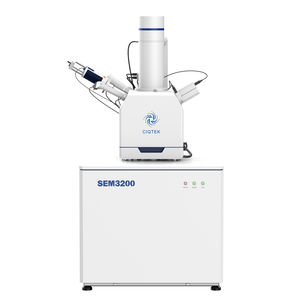
Magnification: 300,000 unit
Resolution: 3, 4, 7 nm
Weight: 480 kg
CIQTEK SEM3200 is a high-performance tungsten filament scanning electron microscope. It has excellent image quality, low vacuum mode compatibility, high resolution images in different fields of view. The depth of field is large and the ...
CIQTEK Co., Ltd.

Magnification: 1 unit - 2,500,000 unit
Resolution: 0.8 nm - 1,200 nm
Weight: 950 kg
CIQTEK SEM5000Pro is a high-resolution, feature-rich field emission scanning electron microscope (FE-SEM, FEG SEM). Advanced column design, high voltage tunneling technology (SuperTunnel), low aberration non-leakage magnetic objective ...
CIQTEK Co., Ltd.
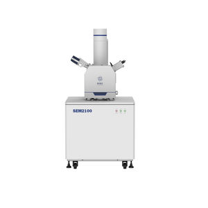
Magnification: 300,000 unit
Resolution: 4.5, 3.9 nm
SEM2100 is a user-friendly and accessible Tungsten Filament Scanning Electron Microscope (SEM) designed for novice users. It features a simplified operating process, and adheres to industry standards and user habits in its User Interface ...
CIQTEK Co., Ltd.
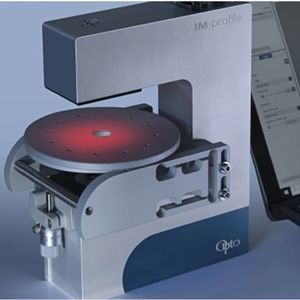
Resolution: 200 nm
Weight: 1 kg
The new Imaging Module profile with 20x 5MP is now also available with a uniquely compact X-Y-Z-Phi table to position the Life Science - Medical sample easily. It is an ultra compact inverse USB/GigE digital microscope with optimized ...

Weight: 17 kg
Length: 490 mm
Width: 251 mm
The ECLIPSE LV100N POL and Ci-POL series of polarising microscopes is used to study the birefringent properties of anisotropic specimens by observing image contrast and colour changes. Nikon offers systems for both quantitative and qualitative ...
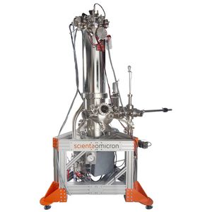
> 5 days uninterrupted measurement time in varying magnetic fields with only 11 L LHe Temperatures down to 1 K with 4He Ultra low thermal drift Magnetic fields BZ > 3 T Optical access STM and QPlus® AFM Ergonomic design & expandable ...
Scienta Omicron

Magnification: 100 unit - 500 unit
Length: 160 mm
In-situ/Field metallography is widely used for microstructure analysis on large parts (samples) that cannot be easily carried or where destructive preparation is not permissible such as storage tanks, piping system, power plants, etc. ...
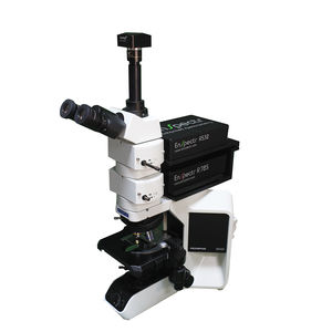
Resolution: 532, 785 nm
Precisely tailored to customer’s requirements Easy to use Fast and trustworthy results Cost-effective fully functional Raman system Low cost system Raman Microscope 532/785® is an optical spectral instrument with specialized ...
enspectr
Your suggestions for improvement:
Receive updates on this section every two weeks.
Please refer to our Privacy Policy for details on how DirectIndustry processes your personal data.
- Brand list
- Manufacturer account
- Buyer account
- Our services
- Newsletter subscription
- About VirtualExpo Group


Please specify:
Help us improve:
remaining