
- Products
- Catalogs
- News & Trends
- Exhibitions
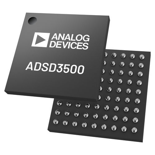
ARM processor ADSD3500signal
Add to favorites
Compare this product
Characteristics
- Type
- ARM
- Other characteristics
- signal
- Clock rate
19.2 MHz, 24 MHz
Description
The ADSD3500 is a Time-of-Flight (ToF) Depth Image Signal Processor (ISP) for Analog Devices ToF products such as the ADTF3175 and ADSD3030. The Depth ISP processes the raw phase frames from the ToF imager, generating the final radial depth, active brightness (AB), and confidence frames. The ADSD3500 supports full computation of depth, active brightness and confidence data for 640x480 resolution, and partial depth computation (pre-phase unwrap) for 1024x1024 resolution. Data and processing flow is controlled using the integrated ARM® Cortex®-M33. Computation is performed using dedicated hardware and memory, enabling a low power ToF depth ISP solution. The ADSD3500 also controls the boot-up of the image sensor module, loading of calibration data, and triggering of frames.
The image data receiver (Rx) and transmitter (Tx) ports use standard Mobile Industry Processor Interface (MIPI) Camera Serial Link 2 (CSI-2) interfaces. Processor programming and operation are controlled through 4-wire QSPI, I2C, and I3C serial interfaces.
The ADSD3500 is available in a 3.47mm x 3.47mm WLCSP, and is specified over an operating temperature range of -25°C to +85°C.
APPLICATIONS
Augmented reality (AR) systems
Robotics
Building automation
Machine vision systems
Features
Depth processor for Analog Devices Time-of-Flight imagers
Full depth processing at 640x480 resolution, up to 90 FPS
Partial depth processing at 1024x1024 resolution, up to 30 FPS
On-chip SRAM for frame buffering & manipulation
Arm Cortex-M33 processor for data flow control
4-lane MIPI CSI-2 receiver interface, 2.5 Gbps per lane
2-lane MIPI CSI-2 transmitter interface, 2.5 Gbps per lane
Catalogs
No catalogs are available for this product.
See all of Analog Devices‘s catalogsExhibitions
Meet this supplier at the following exhibition(s):

Related Searches
- Ethernet switch
- Industrial network switch
- Unmanaged ethernet switch
- Processor
- Multiplexer
- ARM processor
- Multi-channel multiplexer
- Digital data acquisition card
- Analog Devices analog acquisition card
- Signal processor
- Evaluation board
- Dual core processor
- 2 port ethernet switch
- Industrial processor
- Analog multiplexer
- IC modem
- Communication IC modem
- Multiplexer for telecom applications
- RF IC modem
*Prices are pre-tax. They exclude delivery charges and customs duties and do not include additional charges for installation or activation options. Prices are indicative only and may vary by country, with changes to the cost of raw materials and exchange rates.


