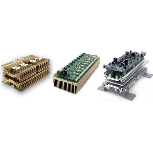
Air Cooled Assemblies
The most efficient way to remove heat from a large area semiconductor (>23mm silicon diameter) is to package it into a flat circular package that allows heat and current to flow from both the anode and cathode of the device with as little thermal and electrical resistance as possible. This type of package is called by many names, hockey puck, press pack, flat pack and disc. From a user’s point of view, it is the most difficult package to use since it not only requires two heat sinks (anode and cathode) but also requires a clamp to hold the assembly together and to apply sufficient force to minimize the thermal and electrical resistance. The proper clamping force ensures optimum electrical and thermal connections to the device. In addition, the method used to tighten and accurately gauge the applied force is not trivial. Over tightening, under tightening and/or not maintaining a parallel force on the pole face of the device often leads to premature device failure. The APS clamp design provides solutions to these problems.
The clamping force applied to the semiconductor pole faces is critical and must adhere to manufacturers specifications. It is also necessary for the clamping force to be applied evenly across the entire surface of both pole faces and normal to the pole face plane of the assembled devices. The clamp must apply the force evenly across the pole faces and not cause mechanical stress to be transferred to the semiconductor element over the entire temperature range to which the assembly will be exposed.


