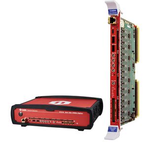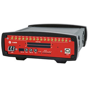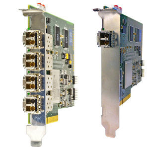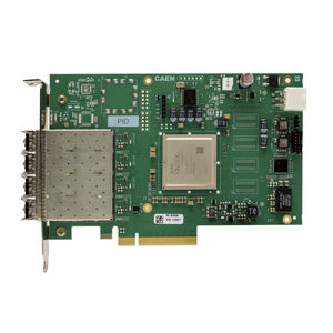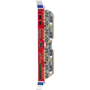
Up to 62.5 MS/s digitizer 64-channel12-bitPCIe
Add to favorites
Compare this product
Characteristics
- Speed
- up to 62.5 MS/s
- Number of channels
- 64-channel
- Options
- 12-bit, PCIe, VME
Description
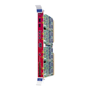
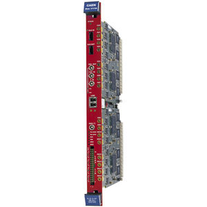
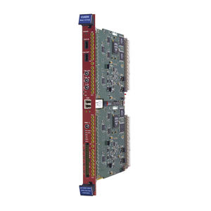
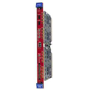
The V1740 is a 1-unit wide VME 6U module housing a 64 Channel 12 bit 62.5 MS/s (65 MS/s using external clock) Flash ADC Waveform Digitizer and featuring 2 Vpp single ended input dynamics on two ERNI SMC connectors. Versions with 10 Vpp (single ended) input full scale range are also available (V1740A/V1740C).
The DC offset adjustment (range ±1 V / 5 V) by programmable 16bit DACs (one for each 8-channel group) allows a right sampling of a bipolar (Vin = ±1 V / 5 V) up to a full positive (Vin = 0 ÷ +2 V / 10 V) or negative (vin = 0 ÷ -2 V / 10 V) analog input swing without losing dynamic resolution.
The module features front panel Clock Input and Output as well as a PLL for clock synthesis from internal/external references. The data stream is continuously written in a circular memory buffer. When the trigger occurs, the FPGA writes further N samples for the post trigger and freezes the buffer that can be read either by VMEbus or Optical Link. The acquisition can continue without dead time in a new buffer.
Each channel has a SRAM Multi-Event Buffer divisible into 1 ÷ 1024 buffers of programmable size. The readout (by VMEbus or Optical Link) of a frozen buffer is independent from the write operations in the active buffer (ADC data storage). Two sizes of the channel digital memory are available by ordering options: 192 kS/ch (mod. V1740/V1740C) and 1.5 MS/ch (mod. V1740A/V1740B).
V1740 supports multi-board synchronization allowing all ADCs to be synchronized to a common clock source and ensuring Trigger time stamps alignment. Once synchronized, all data will be aligned and coherent across multiple V1740 boards.
Catalogs
No catalogs are available for this product.
See all of CAEN Spa‘s catalogs*Prices are pre-tax. They exclude delivery charges and customs duties and do not include additional charges for installation or activation options. Prices are indicative only and may vary by country, with changes to the cost of raw materials and exchange rates.


