- Production Machines
- Other Manufacturing Equipment
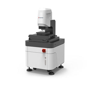
- 3D inspection machine
- Chotest Technology Inc.
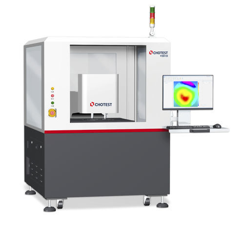
3D inspection machine WD4000for unpatterned wafersfor the electronics industrymeasurement


Add to favorites
Compare this product
Characteristics
- Technology
- 3D
- Applications
- for unpatterned wafers
- Sector
- for the electronics industry
- Other characteristics
- measurement, non-contact
Description
Appliction:
Thickness and warpage measurement for unpatterned wafer
The 3D shape based on the upper and lower surfaces of the wafer is reconstructed by non-contact measurement. The powerful measurement and analysis software ensures the stable calculation for the thickness, roughness, total thickness variation(TTV) of the wafer.
Roughness measurement for unpatterned wafer
During rough grinding and fine grinding process for the Wafer thinning, the surface roughness Sa values and their stability are used to evaluate the processing quality. When the thinned silicon wafer is measured in the strong noise environment of the production workshop, the roughness Sa values of the fine grinding silicon wafers are ranging around 5nm, and the repeatability is 0.046987nm based on 25 times of measurement data which proves the measurement stability is good.
VIDEO
Catalogs

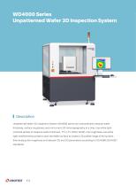
WD4000 SERIES
4 Pages

PRODUCT CATALOGUE
67 Pages
Exhibitions
Meet this supplier at the following exhibition(s):
26th Shenzhen International Industrial Exh.
26-29 Mar 2025 Shenzheng (China) Hall 8 - Stand 8M52
More information
CIMT - China International Machine Tool Show
21-26 Apr 2025 Beijing (China) Hall B5 - Stand 401
More information
Other Chotest Technology Inc. products
Microscopic Surface


*Prices are pre-tax. They exclude delivery charges and customs duties and do not include additional charges for installation or activation options. Prices are indicative only and may vary by country, with changes to the cost of raw materials and exchange rates.