- Products
- Catalogs
- News & Trends
- Exhibitions
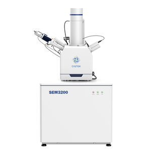
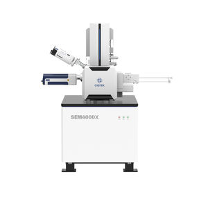
Tungsten filament microscope SEM 3300scanning electronfor analysisfor materials analysis
Add to favorites
Compare this product
Characteristics
- Type
- scanning electron
- Technical applications
- for analysis, for materials analysis, for semiconductors, for geology
- Ergonomics
- upright
- Observation technique
- bright field
- Configuration
- floor-standing
- Electron source
- tungsten filament
- Detector type
- in-lens SE, back-scattered electron
- Options and accessories
- computer-assisted
- Other characteristics
- high-resolution, automatic
- Magnification
Max.: 300,000 unit
Min.: 1 unit
- Resolution
Max.: 5 nm
Min.: 2.5 nm
- Length
926 mm
(36.5 in)- Width
836 mm
(32.9 in)- Height
1,700 mm
(66.9 in)
Description
SEM3300 is a new generation of tungsten filament scanning electron microscope with a resolution better than 2.5 nm @ 20kV. The special electron optics design breaks through the resolution limit of tungsten filament , reaches a resolution of 5 nm at a low voltage of 1 kV.
It has excellent imaging quality, can obtain high- resolution images in various field of view ranges, delivers large depth of field. Great expandability enables to explore the world of microscopic imaging.
Features
1.Resolution:2.5 nm @ 20 kV, SE;4 nm @ 3 kV, SE;5 nm @ 1 kV, SE
2.Magnification:1 ~ 300,000 x
3.Acceleration Voltage:0.1 kV~ 30 kV
4.“SuperTunnel”:Electron Optics Technology
5.Low Voltage High Resolution lmaging:Achieved by Electron Optics Column Beam Deceleration Technology
6.Electromagnetic& Electrostatic Combo Objective Lens:Effectively reduces lens aberration, improves image resolution at low voltages, compatible to imaging of magnetic samples
7.In-column Electron Detection Technology:Improves signal electron capturing efficiency, realizes
high signal-to-noise ratio at high resolution
8.Optical Navigation:Quickly locates targeted samplecoordinates and Regions of Interest(ROI)
9.*AutoMap:Fully automated image acquisition & stitching, mapping a large Field of View
Catalogs
CIQTEK Electron Microscope
15 Pages
Related Searches
- Microscope
- Laboratory microscope
- Inspection microscope
- LED illumination microscope
- Digital camera microscope
- Measuring microscope
- Analysis microscope
- Upright microscope
- USB microscope
- Trinocular microscope
- Bright field microscope
- High-resolution microscope
- Industrial microscope
- Automatic microscope
- Binocular microscope
- Materials research microscope
- Fluorescence microscope
- Quality control microscope
- Medical microscope
- Research microscope
*Prices are pre-tax. They exclude delivery charges and customs duties and do not include additional charges for installation or activation options. Prices are indicative only and may vary by country, with changes to the cost of raw materials and exchange rates.


