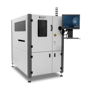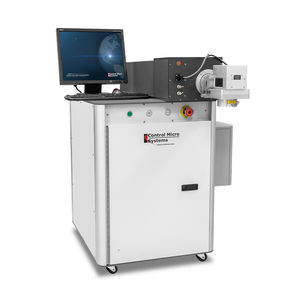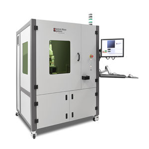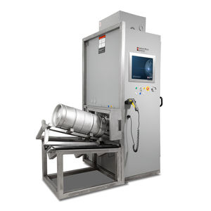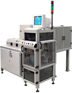
Laser marking machine for PCB

Add to favorites
Compare this product
Characteristics
- Technique
- laser
- Applications
- for PCB
Description
Control Micro Systems we combine our years of experience with a variety of disciplines to provide a turn-key solution: integrating state of the art laser applications with process automation and system validation. By utilizing the wide range of lasers and imaging optics developed by Control Micro Systems we frequently provide our customers with exceptional processing performance and we never lose sight of the ultimate goal of your interest in laser technology improved productivity and lower costs. As such with wafer processing; serialization for traceability, scribing and lapping wafers we offer a range of solutions tailored for your specific requirements. When determining the system offerings we take into account that it must meet many processing requirements such as geometries, dimensions, line width, slag tolerances, and clean room protocol. In addition substrates: silicon, sapphire, compounds (GaAS, InP, SiCO2, SiGe etc.), crystal wafers (LiTaO3 and LiNbO3) or photo resist exposing; of course, handling needs and throughput must be considered when offering the best solution for your needs.
VIDEO
Catalogs
No catalogs are available for this product.
See all of Control Micro Systems‘s catalogsRelated Searches
- Marking machine
- Laser marking workstation
- Metal marking workstation
- Plastic marking workstation
- Automated marking machine
- Fiber laser marking machine
- Laser engraving system
- Aluminum marking workstation
- Integration marking machine
- Air-cooled marking machine
- CO2 laser marking machine
- Paper marking machine
- Marking system
- Wood marking machine
- Glass marking machine
- Programmable marking workstation
- Jewelry marking machine
- Deep marking marking machine
- Printed circuit marking machine
- Computer-controlled marking machine
*Prices are pre-tax. They exclude delivery charges and customs duties and do not include additional charges for installation or activation options. Prices are indicative only and may vary by country, with changes to the cost of raw materials and exchange rates.


