- Electricity - Electronics
- Electronic Component
- CMOS logic gate
- Diodes Incorporated
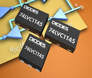
CMOS logic gate 74AUP, 74LVC seriesstandard

Add to favorites
Compare this product
Characteristics
- Options
- CMOS, standard
Description
The Advanced Ultra Low Power (AUP) CMOS logic family is designed
for low power and extended battery life in portable applications.
The 74AUP2G34 is a dual buffer gate with standard push-pull outputs
designed for operation over a power supply range of 0.8V to 3.6V.
The device is fully specified for partial power down applications using
IOFF. The IOFF circuitry disables the output preventing damaging
current backflow when the device is powered down.
Features and Benefits
Advanced Ultra Low Power (AUP) CMOS
Supply Voltage Range from 0.8V to 3.6V
±4mA Output Drive at 3.0V
Low Static power consumption
ICC < 0.9μA
Low Dynamic Power Consumption
CPD = 6pF Typical at 3.6V
Schmitt Trigger Action at All Inputs Make the Circuit Tolerant for Slower Input Rise and Fall Time. The hysteresis is typically 250mV at VCC = 3.0V
IOFF Supports Partial-Power-Down Mode Operation
ESD Protection per JESD 22
Exceeds 200-V Machine Model (A115-A)
Exceeds 2000-V Human Body Model (A114-A)
Exceeds 1000-V Charged Device Model (C101C)
Latch-Up Exceeds 100mA per JESD 78, Class II
Leadless packages per JESD30E
DFN1410 denoted as X2-DFN1410-6
DFN1010 denoted as X2-DFN1010-6
DFN0910 denoted as X2-DFN0910-6
Totally Lead-Free & Fully RoHS Compliant
Halogen and Antimony Free. Green Device
Catalogs
LOGIC PRODUCTS
20 Pages
Related Searches
- Signal amplifying integrated circuit
- Transceiver module
- Rotary electric switch
- Power amplifying integrated circuit
- Diode
- Transistor module
- Rectifier diode
- Electronic amplifying integrated circuit
- On/off electric switch
- LED driver
- Surface-mount diode
- Switching transistor module
- Avalanche diode
- DC amplifying integrated circuit
- MOSFET transistor module
- RF transceiver
- Bipolar transistor
- Portable amplifier
- Adjustable LED driver
- Audio amplifying integrated circuit
*Prices are pre-tax. They exclude delivery charges and customs duties and do not include additional charges for installation or activation options. Prices are indicative only and may vary by country, with changes to the cost of raw materials and exchange rates.


