- Electricity - Electronics
- Electronic Component
- CCD image sensor
- e2v scientific instruments
EMCCD image sensor NIRultravioletvisible
Add to favorites
Compare this product
Characteristics
- Technology
- EMCCD
- Spectrum
- NIR, ultraviolet, visible
Description
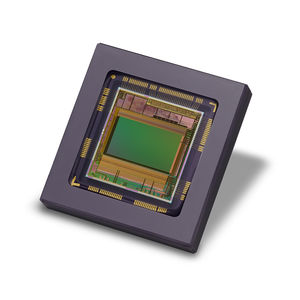
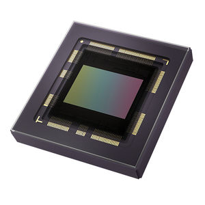
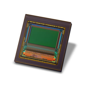
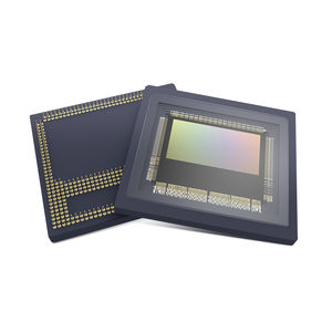
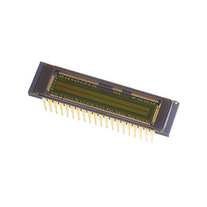
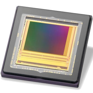
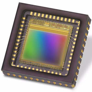
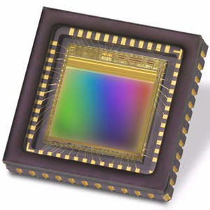
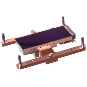
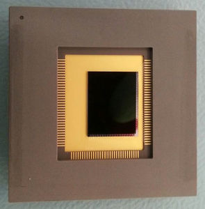
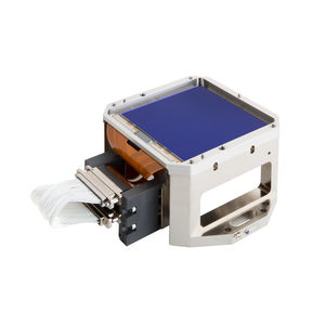
EM (Electron Multiplication) is a technology that uses on-chip gain in the charge domain to effectively eliminate read noise from an image sensor. This enables advanced ultra-low light applications that require extreme sensitivity at fast frame rates. Examples include life science applications such as single molecule detection, super resolution microscopy and spinning disk confocal microscopy along with physical science applications such as nanotechnology imaging, Bose Einstein condensates and soft X-ray spectroscopy, and astronomy applications such as adaptive optics and lucky imaging. The inclusion of an additional conventional output allows further flexibility for applications such as true 24 hour surveillance.
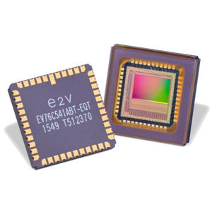
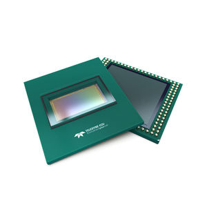
Teledyne e2v EM image sensors are available in a wide range of configurations and can be tailored to the specific needs of the customer. The combination of Teledyne e2v’s back-thinning technology and anti-reflection coatings enables industry leading quantum efficiency that can be optimised for applications in the visible, UV or NIR wavelength ranges. These sensors are also available with shielded anti-blooming, which maintains full well capacity and high quantum efficiency whilst minimising blooming from strong light sources, accompanied by, hermetic packages with thermoelectric coolers to minimise dark signal.
Catalogs
No catalogs are available for this product.
See all of e2v scientific instruments‘s catalogsRelated Searches
- Signal amplifying integrated circuit
- Transceiver module
- RF transceiver
- Microcontroller
- Low-noise amplifying integrated circuit
- CMOS image sensor
- Infrared imaging sensor
- Programmable IC converter
- ADC IC converter
- Low-power transceiver module
- Visible image sensor
- High-speed IC converter
- 32-bit microcontroller
- High-speed image sensor
- DAC IC converter
- Isolation amplifying integrated circuit
- Multi-channel IC converter
- High-sensitivity image sensor
- Near-infrared image sensor
- CCD image sensor
*Prices are pre-tax. They exclude delivery charges and customs duties and do not include additional charges for installation or activation options. Prices are indicative only and may vary by country, with changes to the cost of raw materials and exchange rates.


