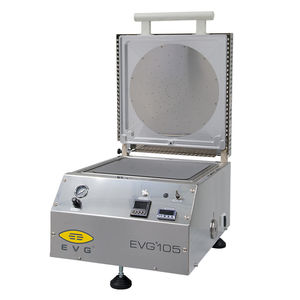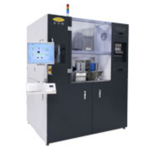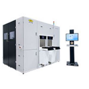
Wafer processing line EVG®101
Add to favorites
Compare this product
Characteristics
- Options
- for wafers
Description
The EVG101 resist processing system performs R&D-type processes on a single chamber design, which is fully compatible with EVG’s automated systems. The EVG101 supports wafers up to 300 mm and can be configured for spin or spray coating and developing. Conformal layers of photoresist or polymers are achieved on 3D structured wafers for interconnection techniques with EVG’s advanced OmniSpray coating technology. This ensures low material consumption of precious high-viscosity photoresists or polymers while improving uniformity and resist spreading options.
Features
Wafer size up to 300 mm
Automated spin or spray coating or developing with manual wafer load/unload
Quick and easy process transfer from research to production utilizing proven modular design and standardized software
Syringe dispense system for utilization of small resist volumes, including high-viscosity resists
Small footprint while maintaining a high level of personal and process safety
Multi-user concept (unlimited number of user accounts and recipes, assignable access rights, different user interface languages)
Options:
Uniform coating of high-topography wafer surfaces with OmniSpray® coating technology
Wax and epoxy coating for subsequent bonding processes
Spin-On-Glass (SOG) coating
*Prices are pre-tax. They exclude delivery charges and customs duties and do not include additional charges for installation or activation options. Prices are indicative only and may vary by country, with changes to the cost of raw materials and exchange rates.


