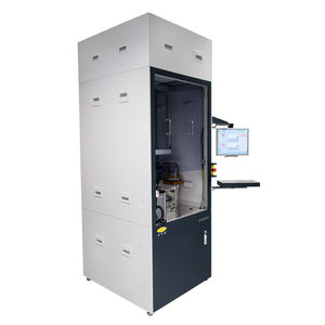
Automated wafer bonder GEMINI®FB
Add to favorites
Compare this product
Characteristics
- Options
- automated
Description
Vertical stacking of semiconductor devices has become an increasingly viable approach to enabling continuous improvements in device density and performance. Wafer-to-wafer bonding is an essential process step to enable 3D stacked devices. EVG's GEMINI FB XT integrated fusion bonding system extends current standards and combines higher productivity with improved alignment and overlay accuracy for applications such as memory stacking, 3D systems on chip (SoC), backside illuminated CMOS image sensor stacking, and die partitioning. The system features the new SmartView NT3 bond aligner, developed specifically for fusion and hybrid wafer bonding alignment requirements of < 50 nm.
Features
New SmartView® NT3 face-to-face bond aligner with sub 50 nm wafer-to-wafer alignment accuracy
Up to six pre-processing modules like:
Clean module
LowTemp™ plasma activation module
Alignment verification module
Debond module
XT Frame concept for highest throughput with EFEM (Equipment Frontend Module)
Optional features:
Debond module
Thermocompression bond module
Technical Data
Wafer diameter (substrate size)
200, 300 mm
Max. number of process modules
6 + SmartView® NT
Optional features
Debond module
Thermocompression bond module
Catalogs
No catalogs are available for this product.
See all of EV Group‘s catalogs*Prices are pre-tax. They exclude delivery charges and customs duties and do not include additional charges for installation or activation options. Prices are indicative only and may vary by country, with changes to the cost of raw materials and exchange rates.


