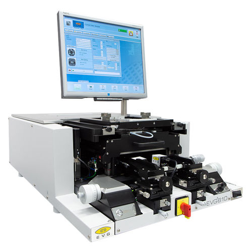
Wafer alignment system EVG®610 BAfor bondingR&DMEMS
Add to favorites
Compare this product
Characteristics
- Applications
- for wafers, for bonding, R&D, MEMS
- Other characteristics
- high-accuracy
Description
The EVG610 bond alignment system is designed for wafer-to-wafer alignment up to 150 mm wafer sizes. EV Group´s bond alignment systems offer a manual high-precision alignment stage with bottom-side microscope. The precision of EVG´s bond alignment system accommodates the most demanding alignment processes in MEMS production and in emerging fields like 3D integration applications.
Features
Most suitable for EVG®501 and EVG®510 bonding systems
Wafer and substrate sizes up to 150 / 200 mm
Manual high-precision alignment stage
Manual-operated bottom-side microscope
Windows® based user interface
Perfect multi-user concept (unlimited number of user accounts, various access rights, different user interface languages)
Desktop system design with minimum footprint
Supports IR alignment process
Optimum total cost of ownership (TCO) for R&D and pilot line production
Technical Data
General system configuration
Desktop
System rack: optional
Vibration isolation: passive
Alignment methods
Backside alignment: ± 2 µm 3 σ
Transparent alignment: ± 1 µm 3 σ
IR alignment: option
Alignment stage
Precision micrometers: manual
Optional: motorized micrometers
Wedge compensation: automated
Catalogs
No catalogs are available for this product.
See all of EV Group‘s catalogs*Prices are pre-tax. They exclude delivery charges and customs duties and do not include additional charges for installation or activation options. Prices are indicative only and may vary by country, with changes to the cost of raw materials and exchange rates.

