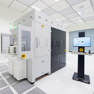
UV-NIL lithography system EVG®7300
Add to favorites
Compare this product
Characteristics
- Type
- UV-NIL
Description
New Multi-Functional Micro- and Nanoimprint Solution from EV Group Offers Unprecedented Flexibility for High-Volume Optical Device Manufacturing
EVG®7300 is the most advanced EVG solution to combine multiple UV-based processes, such as nanoimprint lithography (NIL), lens molding and lens stacking (UV bonding), in a single platform
The EVG®7300 SmartNIL® nanoimprint and wafer-level optics system is a versatile, advanced solution that combines multiple UV-based process capabilities in a single platform.
EV Group (EVG), a leading supplier of wafer bonding and lithography equipment for the MEMS, nanotechnology and semiconductor markets, today introduced the EVG®7300 automated SmartNIL® nanoimprint and wafer-level optics system. The EVG7300 is the company’s most advanced solution to combine multiple UV-based process capabilities, such as nanoimprint lithography (NIL), lens molding and lens stacking (UV bonding), in a single platform. This industry-ready, multi-functional system is designed to serve advanced R&D and production needs for a wide range of emerging applications involving micro- and nano-patterning as well as functional layer stacking. These include wafer-level optics (WLO), optical sensors and projectors, automotive lighting, waveguides for augmented reality headsets, bio-medical devices, meta-lenses and meta-surfaces, and optoelectronics. Supporting wafer sizes up to 300 mm and featuring high-precision alignment, advanced process control and high throughput, the EVG7300 meets the high-volume manufacturing needs for a variety of freeform and high-precision nano- and micro-optical components and devices.
Catalogs
No catalogs are available for this product.
See all of EV Group‘s catalogs*Prices are pre-tax. They exclude delivery charges and customs duties and do not include additional charges for installation or activation options. Prices are indicative only and may vary by country, with changes to the cost of raw materials and exchange rates.


