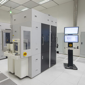
Wafer metrology system EVG®40 NT2
Add to favorites
Compare this product
Characteristics
- Type
- for wafers
Description
EV Group Brings High-Speed High-Precision Metrology to 3D Heterogeneous Integration
EVG®40 NT2 offers breakthrough metrology performance to accelerate implementation of wafer- and die-level hybrid bonding and maskless lithography
EV Group (EVG), a leading supplier of wafer bonding and lithography equipment for the MEMS, nanotechnology and semiconductor markets, today unveiled the EVG®40 NT2 automated metrology system, which provides overlay and critical dimension (CD) measurements for wafer-to-wafer (W2W), die-to-wafer (D2W) and die-to-die (D2D) bonding as well as maskless lithography applications. Designed for high-volume production with feedback loops for real-time process correction and optimization, the EVG40 NT2 helps device manufacturers, foundries and packaging houses accelerate the introduction of new 3D/heterogeneous integration products as well as improve yields and avoid scrapping of highly valuable wafers.
EVG will showcase the EVG40 NT2 system for the first time at the SEMICON Europa tradeshow, taking place November 16-19 at the Messe München in Munich, Germany. Attendees interested in learning more can visit EVG in Hall B1, booth B1460.
As traditional 2D silicon scaling reaches its cost limits, the semiconductor industry is turning to heterogeneous integration—the manufacturing, assembly and packaging of multiple different components or dies with different feature sizes and materials onto a single device or package—in order to increase performance on new device generations. In W2W, D2W and D2D bonding, tight alignment and overlay accuracy is required to achieve good electrical contact between the interconnected devices.
Catalogs
No catalogs are available for this product.
See all of EV Group‘s catalogs*Prices are pre-tax. They exclude delivery charges and customs duties and do not include additional charges for installation or activation options. Prices are indicative only and may vary by country, with changes to the cost of raw materials and exchange rates.


