Temperature measurement system IMS-K-Powerfor wafersfor semiconductorsrugged
Add to favorites
Compare this product
Characteristics
- Measured physical value
- temperature
- Measured material
- for wafers, for semiconductors
- Other characteristics
- rugged
Description
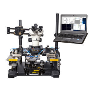
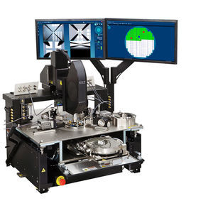
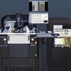
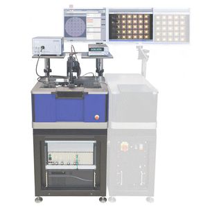
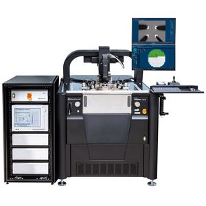
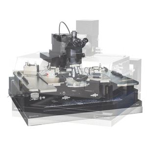
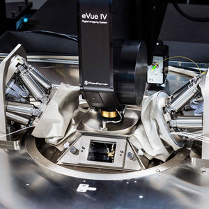
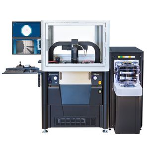
Comprehensive, Turn-key Integrated Measurement System (IMS) with Keysight PDA
for On-wafer R&D Power Semiconductor Device Characterization Measurements
FormFactor and partner Keysight applications experts will help you configure a robust, complete solution, including:
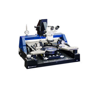
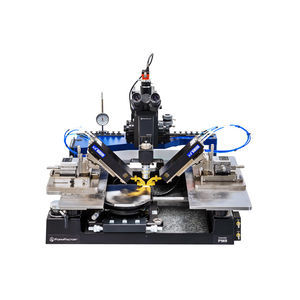
• FormFactor probe system: TESLA300, TESLA200, T200, EPS150TESLA (others available)
• Manual, semi-automatic and fully automatic probes station options
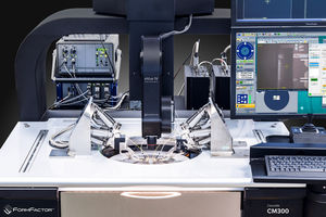
• FormFactor analytical probes: High Voltage Probes, High Current Probes, High-Power Probes
• T.I.P.S. “LuPo” High Voltage / High Power Probe Card (optional)
• Full over temperature measurements and automation from -60°C to +300°C
• Keysight power device analyzer (PDA): B1505A (others available)
• Keysight automation and modeling software: EasyEXPERT group+
• To complete the system: cables, adapters, mounting hardware, etc.
Industry’s Most Productive and Accurate Power Semiconductor Device Characterization System
When testing Si and advanced GaN / SiC devices on-wafer instead of in-package, R&D engineers and test operators are faced with some major challenges to collect high accuracy data. These include the need for probe and system anti-arcing at high voltage, low resistance probe and wafer contacts for high current, and special handling for thinned wafers.
Catalogs
No catalogs are available for this product.
See all of FORMFACTOR‘s catalogsRelated Searches
- Measuring machine
- Optical measuring machine
- Automatic measuring machine
- Laser scanning system
- High-precision measuring machine
- 3D measuring machine
- Compact measuring machine
- Thickness measurement system
- Calibration measuring machine
- High-speed measuring machine
- Rugged measuring machine
- Shape measuring machine
- High-resolution measuring machine
- Temperature measurement system
- Wafer measurement system
- Roughness measuring machine
- Flatness measuring machine
- Automated scanning system
- Fully-automatic measuring machine
- Non-destructive measuring machine
*Prices are pre-tax. They exclude delivery charges and customs duties and do not include additional charges for installation or activation options. Prices are indicative only and may vary by country, with changes to the cost of raw materials and exchange rates.


