- Metrology - Laboratory
- Laboratory Equipment
- Electron microscope
- Hitachi High-Tech Europe GmbH
- Products
- Catalogs
- News & Trends
- Exhibitions
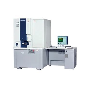
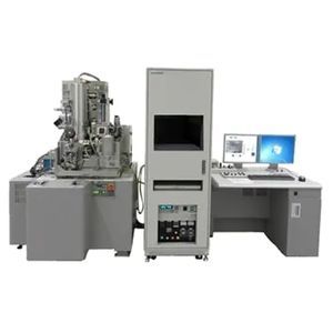
Electron microscope NE4000for analysiscold field emissionCCD

Add to favorites
Compare this product
Characteristics
- Type
- electron
- Technical applications
- for analysis
- Electron source
- cold field emission
- Detector type
- CCD
- Other characteristics
- observation, piezoelectric, for nanotechnology, high-precision
Description
The Hitachi NE4000 nanoEBAC is an electron beam based probing system for electrical characterization and EBAC analysis and imaging of microelectronic device interconnects, materials, and components.
Electron Beam Absorbed Current (EBAC) technique offers a quick and effective method to identify open circuits, high resistance and shorts along interconnects without direct probing techniques of lower level layers.
The EBAC technique is performed with the electron beam by passing through the dielectric layers down to the lower level metallization layer in order to absorb the electron beam current. The electron beam accelerating voltage of the FESEM controls the probing depth or penetration level through the dielectric layers. A single probe is placed on the exposed, upper layer metallization to complete the circuit and allow the electrons to flow through the interconnect.
Observation of high resistance and shorts due to Seebeck effect is possible by using dual probes along with the Hitachi patented differential EBAC amplifiers.
User-Friendly Design
• Intuitive GUI(Graphical User Interface) with various image and color processing functions.
• Coarse positioning of probes are accomplished by an integrated in-chamber CCD camera system.
Premium Image Quality
• Provides high quality EBAC images with Hitachi's patented high performance EBAC amplifiers.
Catalogs
No catalogs are available for this product.
See all of Hitachi High-Tech Europe GmbH‘s catalogsOther Hitachi High-Tech Europe GmbH products
Electron Microscopes (SEM/TEM/STEM)


Related Searches
- Hitachi microscope
- Hitachi laboratory microscope
- Inspection microscope
- Tabletop microscope
- Digital camera microscope
- Measuring microscope
- Hitachi analysis microscope
- Bright field microscope
- Hitachi high-resolution microscope
- Industrial microscope
- Hitachi automated microscope
- Compact microscope
- Metallurgical microscope
- Materials research microscope
- Quality control microscope
- Research microscope
- Black field microscope
- Ergonomic microscope
- Hitachi sample preparation system
- 3D microscope
*Prices are pre-tax. They exclude delivery charges and customs duties and do not include additional charges for installation or activation options. Prices are indicative only and may vary by country, with changes to the cost of raw materials and exchange rates.