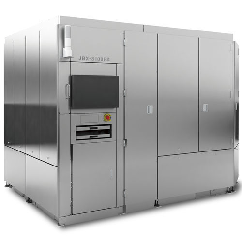
Spot type Electron Beam Lithography System JBX-8100FS achieved high throughput, small footprint and electric power saving.
Features
Small footprint
The area required for the standard system is 4.9 m (W) x 3.7 m (D) x 2.6 m (H), much smaller than the conventional systems.
Low power consumption
Power needed for normal operation is approximately 3 kVA, reduced to 1/3 of the conventional systems.
High throughput
The system has two exposure modes, high resolution and high throughput modes, supporting different types of patterning from ultra fine processing to small to mid size production. It has minimized the idle time during exposure while increasing the maximum scanning speed by 1.25 to 2.5 times to 125 MHz (the world’s highest level) for high speed writing.
Version
The JBX-8100FS is available in 2 versions: G1 (entry model) and G2 (full option model). Optional accessories can be added to the G1 model as needed.
New Functions
An optional optical microscope is available to enable examination of patterns on the sample without exposing resist to light. A signal tower is provided as standard for visual monitoring of system operation.
Laser positioning resolution
Stage positions are measured and controlled in 0.6 nm steps as standard, and in 0.15 nm steps with an optional upgrade.
System control
Versatile Linux® operating system combined with a new graphic user interface provides ease in operation. The data preparation program supports both Linux® and Windows®.

