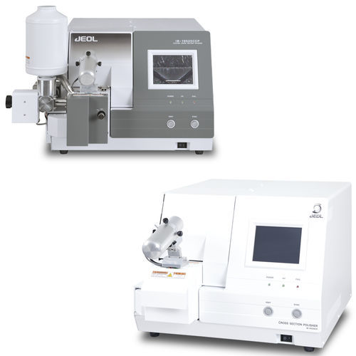
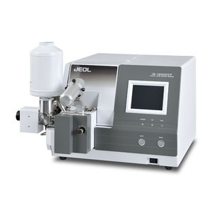
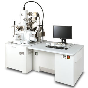
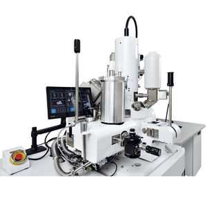
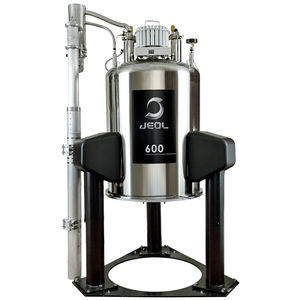
Automatic sample preparation system IB-10500HMSfor the laboratoryfor SEMion beam milling

Add to favorites
Compare this product
Characteristics
- Operation
- automatic
- Applications
- for the laboratory, for SEM
- Preparation type
- ion beam milling
Description
Features
High Throughput Milling *1
High milling rate of cross-section achieved by the new ion source:1.2mm/h or more*2
(2.4 times than the previous milling rate.)
The high throughput milling system optimizes the ion source electrodes and enables higher accelerating voltages, thus improving the ion-beam current density.
Our newly developed ion source achieves a high milling rate of cross-section of 1.2 mm/h or more (2.4 times than the previous milling rate.)
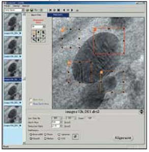
Cross-section milling rate of the new ion source
Specimen: Silicon wafer
Accelerating voltage: 10kV
Milling time: 1h
Cross-section milling of a low melting-point alloy (cooling)
Accelerating voltage: 10 kV
Milling time: 30 min
The right SEM image shows an Sn-Bi alloy with a melting point of 150°C.
A low melting-point metal can be melted due to the processing heat; therefore, cooling of the metal is required before milling. High throughput milling is applied to the heat-sensitive specimen while the specimen is kept cooled *3.
Then, a cross-section specimen with a reduced heat damage is obtained in a short time.
Large Area Milling *1,*4
Planar Surface Milling of Larger Area
The new high throughput milling system has enabled the irradiation of an ion beam onto a larger area of the specimen.
Planar surface milling is effective to remove scratches generated on the specimen surface or crystalline strains, which are caused by mechanical polishing.
Planar surface milling of a concrete
Accelerating voltage: 10 kV
Milling time: 20 min
Large-area planar surface milling was applied to a concrete with a width of 20mm.
Catalogs
No catalogs are available for this product.
See all of Jeol‘s catalogsOther Jeol products
Scientific Instruments


Related Searches
- Jeol microscope
- Jeol laboratory microscope
- Tabletop microscope
- Digital camera microscope
- Jeol analysis microscope
- Bright field microscope
- Jeol high-resolution microscope
- Industrial microscope
- Jeol automated microscope
- Compact microscope
- Medical microscope
- Fluorescence microscope
- Black field microscope
- Specimen maker
- 3D microscope
- Jeol electron microscope
- Automatic sample preparation system
- Jeol observation microscope
- Real-time microscope
- High-speed microscope
*Prices are pre-tax. They exclude delivery charges and customs duties and do not include additional charges for installation or activation options. Prices are indicative only and may vary by country, with changes to the cost of raw materials and exchange rates.