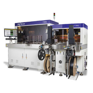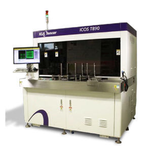
3D inspection system Kronos™ 1190AIautomaticfor the packaging industry
Add to favorites
Compare this product
Characteristics
- Technology
- 3D, AI
- Operational mode
- automatic
- Applications
- for the packaging industry
- Product applications
- for wafers
Description
The Kronos™ 1190 patterned wafer inspection system with high resolution optics provides best in class sensitivity to critical defects for process development and production monitoring in advanced wafer-level packaging (AWLP) applications including 3D IC and high-density fan-out (HDFO). DefectWise™ integrates Artificial Intelligence (AI) as a system level solution, delivering a large boost in sensitivity, productivity and classification accuracy to address the challenges of overkill and defect escapes. DesignWise™ refines the FlexPoint™ precisely targeted inspection areas with direct design input to further reduce nuisance. Supporting bonded, thinned, warped and diced substrates, the Kronos 1190 system enables cost-effective defect inspection down to 150nm in critical process steps like post-dicing, pre-bonding, patterning of Cu pads, Cu pillars, bumps, through silicon vias (TSVs) and redistribution layers (RDL).
Applications
Defect discovery, Process debug, Process monitor, Tool monitor, Outgoing Quality Control (OQC)
Catalogs
No catalogs are available for this product.
See all of KLA Corporation‘s catalogsRelated Searches
- Inspection system
- Measurement monitoring device
- Inspection machine
- Automated inspection system
- Real-time monitoring device
- Temperature monitoring device
- Process monitoring device
- Automatic inspection machine
- Industrial inspection machine
- Surface inspection system
- Defect detection inspection system
- Defect inspection machine
- Optical inspection system
- Optical inspection machine
- Fast inspection system
- 3D inspection system
- Production inspection system
- Measurement inspection machine
- Surface inspection machine
- Inspection system for the packaging industry
*Prices are pre-tax. They exclude delivery charges and customs duties and do not include additional charges for installation or activation options. Prices are indicative only and may vary by country, with changes to the cost of raw materials and exchange rates.


