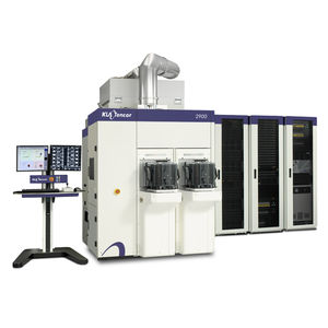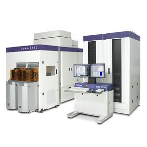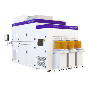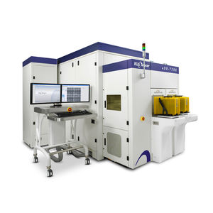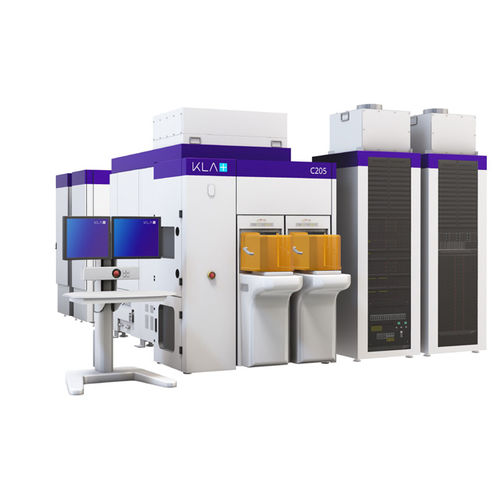
Optical inspection machine C205for patterned wafersfor the electronics industrydefect
Add to favorites
Compare this product
Characteristics
- Technology
- optical
- Applications
- for patterned wafers
- Sector
- for the electronics industry
- Other characteristics
- defect
Description
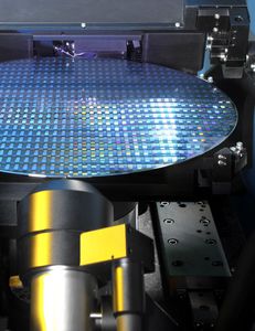
The C205 broadband plasma optical defect inspection system enables systematic defect discovery and latent reliability defect detection for chip manufacturing for the automotive, IoT, 5G and consumer electronics markets. The C205 leverages a tunable broadband illumination source, advanced optics and a low noise sensor to capture systematic defects, helping accelerate characterization and optimization of new processes, design nodes and devices during R&D. NanoPoint™ technology focuses inspection on pattern areas at high risk for reliability failures, delivering actionable defect data that helps reduce die overkill. In production, the C205 monitors critical layers requiring high sensitivity, helping fabs avoid defect excursions that affect final chip quality. The C205 is an extendible, configurable platform supporting both 200mm and 300mm wafer sizes.
Defect discovery, Hotspot discovery, Process debug, Engineering analysis, Line monitoring, Process window discovery
Catalogs
*Prices are pre-tax. They exclude delivery charges and customs duties and do not include additional charges for installation or activation options. Prices are indicative only and may vary by country, with changes to the cost of raw materials and exchange rates.


