
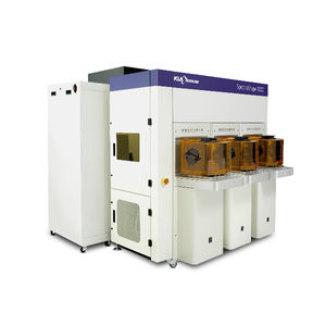
Thickness measuring system PWG™shapeflatness3D

Add to favorites
Compare this product
Characteristics
- Measured physical value
- thickness, shape, flatness
- Technology
- 3D
- Measured material
- for wafers
- Applications
- for electronics
Description
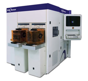
The PWG™ patterned wafer metrology platform produces full wafer dense shape, comprehensive wafer flatness and dual-sided nanotopography data for advanced 3D NAND, DRAM and logic manufacturers. PWG5™, with high resolution and high-density sampling, measures stress-induced wafer shape changes, wafer shape-induced pattern overlay errors, wafer thickness variations and wafer front and backside topography. With industry-best dynamic range, the PWG5 supports inline monitoring and control of wafer warp and stress resulting from deposition processes used to fabricate the 96+ layer stacks of advanced 3D NAND devices. The PWG5 identifies process-induced wafer shape variations at the source, enabling re-work of the wafer, re-calibration of a process tool or integration with KLA’s 5D Analyzer® data analytics system to feed results to the scanner to improve on-product overlay and overall device yield.
Applications
Process monitoring, Inline monitoring, Lithography overlay control
PWG5™ with XT Option
Additional technologies extend the wafer handling and measurement capabilities of the PWG5 patterned wafer geometry system to support wafer-to-wafer bonding measurements for advanced wafer-level packaging applications.
PWG3™
Third-generation patterned wafer geometry measurement system, supporting inline monitoring of fab-wide processes for a range of memory and logic device types at the 2X/1Xnm design nodes.
Catalogs

Other KLA Corporation products
Metrology


Related Searches
- Test machine
- Measuring machine
- Tensile test machine
- Optical measuring machine
- Automatic measuring machine
- High-precision measuring machine
- Control measuring machine
- Tension and compression testing machine
- Manual test machine
- Surface measuring machine
- Dimensional measuring machine
- Industrial profiler
- 3D measuring machine
- Thickness measurement system
- Electronic measuring machine
- Shape measuring machine
- High-temperature testing machine
- Optical profiler
- Temperature measurement system
- 3D profiler
*Prices are pre-tax. They exclude delivery charges and customs duties and do not include additional charges for installation or activation options. Prices are indicative only and may vary by country, with changes to the cost of raw materials and exchange rates.