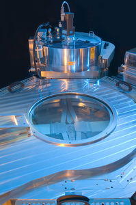
PECVD deposition machine Delta™for packaging
Add to favorites
Compare this product
Characteristics
- Method
- PECVD
- Applications
- for packaging
Description
Plasma Enhanced Chemical Vapor Deposition (PECVD) is a process which uses the energy within the plasma to accelerate chemical reactions at the wafer surface to produce thin films at temperatures below 400°C. Energetic ion bombardment during deposition can be used to tailor the films’ electrical and mechanical properties. The SPTS Delta™ PECVD systems are used for a wide range of applications within the advanced packaging, RF, power, photonics and MEMS markets, particularly in applications where a low processing temperature is required. The Delta™ fxP cluster system offers a comprehensive library of processes for a wide range of dielectric films and with deposition temperatures from 80°C to 400°C. The system also offers single and multi-wafer preheat chamber options for de-gassing sensitive substrates and edge contact processing capability for wafer back side deposition.
• SiCN for hybrid bonding & thick SiO for inter-die gapfill
• TSV liners and via-reveal passivation
• SiN passivation for power chips with low power, low damage option for GaN
• Low temperature back side films with bow compensation
• Highly uniform SiN for MIM capacitor and GaAs device passivation.
• Tuned RI and doped films for active and passive photonics
Catalogs
No catalogs are available for this product.
See all of KLA Corporation‘s catalogs*Prices are pre-tax. They exclude delivery charges and customs duties and do not include additional charges for installation or activation options. Prices are indicative only and may vary by country, with changes to the cost of raw materials and exchange rates.


