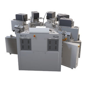
PVD deposition machine Sigma®sputteringthin-filmfor packaging
Add to favorites
Compare this product
Characteristics
- Method
- PVD
- Technology
- sputtering
- Deposition type
- thin-film
- Applications
- for packaging
Description
Physical Vapor Deposition (PVD) is a thin-film process that produces coatings of conducting, semiconducting or insulating materials onto a wafer surface. There are different forms of PVD: sputtering, evaporation, ion-beam deposition. KLA offers products based on sputtering technology. In the sputtering process, a "target" provides the source material that is bombarded with ions from a plasma in the process chamber. Atoms of the source material are ejected or sputtered into the plasma where reactions may or may not take place (depending on the process gas mix) and then condense onto the wafer surface. The SPTS Sigma® PVD system supports wafer sizes from 100mm to 300mm, and the fxP cluster platform allows integration of different forms of pre-treatment and deposition technology, depending on the specific process requirements.
• Single wafer processing, improves yields and on-wafer performance, compared with batch processing.
• Planar target with full-face erosion
• Rapid target change, increases uptime
• Reliable handling of fragile, thinned or bowed wafers
• “Super Uniformity” option available for specialist applications
• Multi-wafer degas to increase throughput for long (low temp) degas applications
Catalogs
ICOS™ T3/T7
4 Pages
ICOS™ T890
4 Pages
*Prices are pre-tax. They exclude delivery charges and customs duties and do not include additional charges for installation or activation options. Prices are indicative only and may vary by country, with changes to the cost of raw materials and exchange rates.


