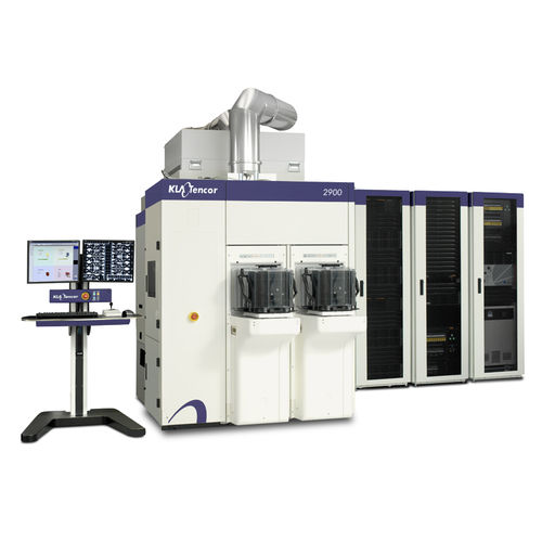
The 2965 and 2950 EP broadband plasma defect inspection systems provide advancements in optical defect inspection, enabling discovery of yield-critical defects on ≤5nm logic and leading-edge memory design nodes. Using enhanced broadband plasma illumination technologies, such as Super•Pixel™ mode and advanced detection algorithms, the 2965 and 2950 EP inspectors provide the sensitivity required to capture critical defects across a range of process layers, material types and process stacks. With a wavelength band that enables capture of critical nanosheet defects, the 2965 enables chip manufacturers to ramp and produce leading-edge chips with gate all around transistor architectures. The 2950 EP includes several hardware, algorithm and defect binning innovations that support defect discovery and monitoring for 3D NAND and DRAM devices. As the industry-standard for inline monitoring, the 2965 and 2950 EP pair sensitivity with optical wafer defect inspection speed, enabling Discovery at the Speed of Light™ – the combination of fast defect discovery and full characterization of defect issues at optimal cost of ownership.
• Tunable DUV, UV, visible broadband illumination source, with new spectral filter
• Selectable optical apertures
• Low-noise sensor
• Super•Pixel™ inspection test mode for high throughput at sensitivity
• Advanced defect detection algorithms, including MCAT
• iDO™ 3.0 with advanced machine learning techniques for defect binning and nuisance suppression
• Novel algorithms for capture of critical defects of interest at the edges of memory cells and for binning of defects at critical memory process steps


