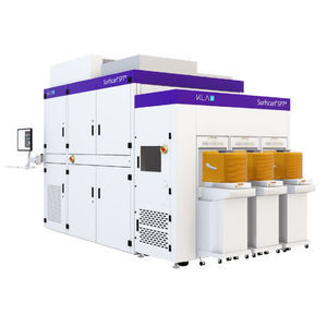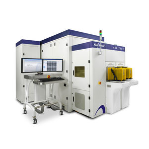
Optical inspection system 8 seriesscanningfor the automotive industryfor the electronics industry


Add to favorites
Compare this product
Characteristics
- Technology
- optical, scanning
- Applications
- for the automotive industry, for the electronics industry
- Product applications
- for wafers
- Configuration
- custom
- Other characteristics
- fast, LED
Description
High Productivity Patterned Wafer Broad Range Inspection Systems
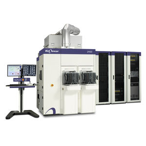
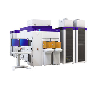
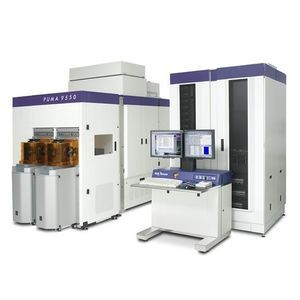
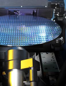
The 8 Series patterned wafer inspection systems detect a wide variety of defect types at very high throughput for fast identification and resolution of production process issues. The 8 Series provides cost-effective defect monitoring for chip manufacturing using 150mm, 200mm or 300mm silicon, SiC, GaN, glass and other substrates, from initial product development through volume production. The latest generation 8935 inspector employs new optical technologies and DesignWise® and FlexPoint™ precise area inspection techniques to capture critical defects that can cause chip failures. DefectWise® AI technology enables fast, inline separation of defect types for improved defect discovery and binning. With these innovations, the 8935 supports high productivity capture of yield and reliability-related defects at a low nuisance rate, helping chip manufacturers accelerate delivery of their products—reliably and at lower cost. The 8 Series inspectors support defect monitoring during fabrication of a broad range of leading-edge and legacy node device types, including logic, memory, power devices, LED, photonics, RF devices and MEMS. The 8 Series systems also support quality control during production of AR/VR lenses and hard disk drive (HDD) manufacturing.
Applications
Process monitor, Tool monitor, Outgoing Quality Control (OQC)
Catalogs
No catalogs are available for this product.
See all of KLA Corporation‘s catalogsRelated Searches
- Inspection system
- Measurement monitoring device
- Inspection machine
- Automated inspection system
- Real-time monitoring device
- Temperature monitoring device
- Process monitoring device
- Automatic inspection machine
- Industrial inspection machine
- Surface inspection system
- Defect detection inspection system
- Defect inspection machine
- Optical inspection system
- Fast inspection system
- 3D inspection system
- Production inspection system
- Inspection system for the packaging industry
- Optical inspection machine
- Measurement inspection machine
- Inspection machine for the electronics industry
*Prices are pre-tax. They exclude delivery charges and customs duties and do not include additional charges for installation or activation options. Prices are indicative only and may vary by country, with changes to the cost of raw materials and exchange rates.


