
- Products
- Catalogs
- News & Trends
- Exhibitions
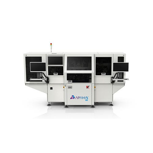
Automatic packaging machine APAMA C2Sline-typetabletfor laboratories
Add to favorites
Compare this product
Characteristics
- Operational mode
- automatic
- Type
- line-type
- Applications
- tablet
- Domain
- for laboratories
- Other characteristics
- multipack
Description
The APAMA Chip-to-Substrate (C2S) offers fully Automated solution for Thermo-
Compression Bonding (TCB), High Density Fan-Out Wafer Level Packaging (HD FOWLP) and High Accuracy Flip Chip (HA FC).
Cost-of-Ownership Advantage
Modular designs allow the flexibility of upgrading from HD FOWLP or HA FC to TCB processes enabling effective cost-of-ownership and preserving the investments of our customers.
C2S Features & Benefits:
Automation
Control
Placement Accuracy
Performance
Yield Enhancement
Adaptability
Cost-of-Ownership Advantage
Enterprise & Consumer Applications
Network Routers and Switches
Servers
High-end PCs and Graphics
Smartphones and Tablets
*Prices are pre-tax. They exclude delivery charges and customs duties and do not include additional charges for installation or activation options. Prices are indicative only and may vary by country, with changes to the cost of raw materials and exchange rates.


