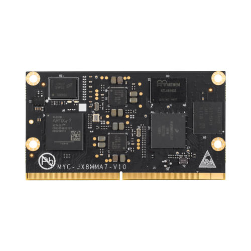
MYC-JX8MMA7 SOM and development board are based on ARM+FPGA architecture, FPGA end is used to realize high-speed data acquisition and processing, ARM end is used to realize data processing, control, communication and display.
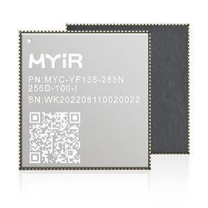
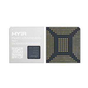
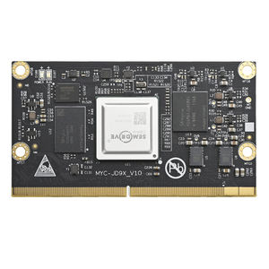
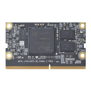
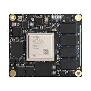
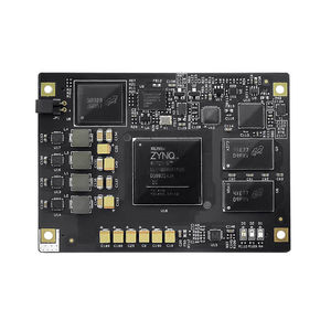
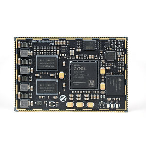
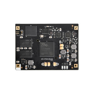
Measuring 82mm by 45mm, the MYC-JX8MMA7 SOM adopts the processing architecture of ARM+FPGA embedded system. It is a compact System-On-Module (SOM) based on 1.8GHz NXP i.MX 8M Mini quad-core ARM Cortex-A53 plus 400MHz Cortex-M4 processor and an integrated Xilinx XC7A25T Artix-7 FPGA. The SOM takes full advantages of the ARM MPU to provide powerful multimedia capability for data processing, control, communication and display, as well as enough FPGA resources for high-speed data acquisition, processing and AD module expansion.
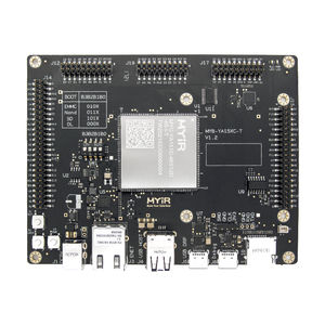
The MYD-JX8MMA7 development board provides a complete evaluation platform for the SOM. A plenty of peripherals interfaces are carried out to the base board like two USB Host and one OTG, one Gigabit Ethernet, two SFP network interfaces, WiFi/Bluetooth module interface, USB 2.0 based M.2 Key B 5G Module interface, LVDS and HDMI display interfaces, MIPI and Parallel CSI interfaces, Audio, one 2x 20-pin UART/I2C/SPI/GPIO extension header which is compatible with Raspberry Pi interface, etc.
The software information for the MYC-JX8MMA7 SOM and development board includes, but is not limited to, U-boot, Linux, all peripheral driver source code, and QT5-based MEasy HMI V2.0 system-related development tools. The documentation comprises product manuals, hardware user manuals, hardware design guides, baseboard PDF schematic diagrams, as well as Linux software evaluation and development guides