- Production Machines
- Cutting Machine
- Laser cutting machine
- New Wave Research
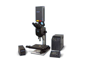
Laser cutting machine 9900for plasticswaferCNC
Add to favorites
Compare this product
Characteristics
- Technology
- laser
- Material
- for plastics
- Product handled
- wafer
- Control type
- CNC
Description
ESI’s 9900 system is revolutionary for the semiconductor industry as it enables our customers to fully adopt 3D integration into their high volume manufacturing environments. Optimized for high precision and speed, the 9900 delivers:
* Advanced technology in one integrated system – The 9900 enables full-cut dicing of ultra-thin wafers and scribing logic or system on chip (SoC) wafers on die attach films (DAFs) in one integrated system.
* Unparalleled die break strength – Some wafers have delicate, brittle, low k materials on the topmost layers of the wafer. Cutting through this without damage is critical. The 9900 uses a proprietary laser and dry etch process to maximize die strength for the most challenging applications.
* Increased precision and yields – The 9900 uses a precision-controlled laser with 355nm wavelength output to the ultra-thin wafer surface. This enables manufacturers to minimize scribe line widths and produce more die per wafer.
* Optimized run rates – The easy-to-use software and recipe library allow customers to optimize run rates for their specific manufacturing applications.
Catalogs
No catalogs are available for this product.
See all of New Wave Research‘s catalogs*Prices are pre-tax. They exclude delivery charges and customs duties and do not include additional charges for installation or activation options. Prices are indicative only and may vary by country, with changes to the cost of raw materials and exchange rates.


