
- Products
- Catalogs
- News & Trends
- Exhibitions
X-ray inspection machine XT V 160CTPCBfor the electronics industry


Add to favorites
Compare this product
Characteristics
- Technology
- X-ray, CT
- Applications
- PCB
- Sector
- for the electronics industry
- Other characteristics
- measurement, automatic, automated
- Output power
20 W
(0 hp)- Convey weight capacity
5 kg
(11 lb)
Description
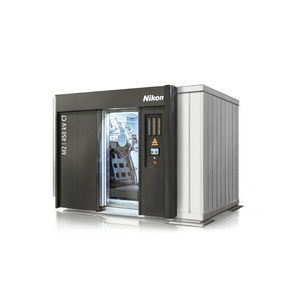
Nikon’s XT V range comprises world-class X-ray and CT systems for non-destructive inspection of electronic components (PCBs, BGAs, chips and much more).
With sub-micron feature recognition, the XT V system range meets today’s need for high performance, non-destructive inspection of complex electronic components. Nikon’s Xi Nanotech X-ray source paired with industry leading flat panel detectors produces best-in-class image quality, with seamless transition between 2D and 3D inspection.
Superior X-Ray Source
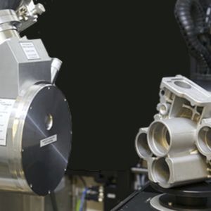
Nikon’s market-leading Xi Nanotech X-ray microfocus source is unique due to its exclusive integral generator design and unparalleled 160kV maximum energy and 20W true-target power.
PCB Analysis Suite
PCB Analysis Suite is capable of advanced measurement and analysis of BGA, bond wires, PTH and complex packages such as PoP on multi-layered boards, with automated pass/fail inspection and reporting.
Oblique Angle Concentric Imaging
Extreme oblique angle field of view up to 90°, with 360° sample rotation, maintains the region of interest thanks to intelligent software and hardware.
VIDEO
Catalogs
Related Searches
- Nikon Metrology measuring system
- Micrometer
- Optical measuring machine
- Nikon Metrology automatic measuring system
- Inspection machine
- Laser scanning system
- Measurement scanning system
- 3D scanning system
- Nikon Metrology high-precision measuring system
- Nikon Metrology measuring system for industrial applications
- Nikon Metrology parts measuring system
- Control measuring machine
- Distance measuring machine
- Non-contact measuring machine
- Digital micrometer
- Diameter measuring machine
- Nikon Metrology laser measuring system
- Nikon Metrology video measuring system
- Inspection scanning system
- High-resolution scanning system
*Prices are pre-tax. They exclude delivery charges and customs duties and do not include additional charges for installation or activation options. Prices are indicative only and may vary by country, with changes to the cost of raw materials and exchange rates.


