
- Products
- Catalogs
- News & Trends
- Exhibitions
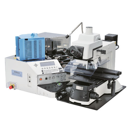
Automatic materials handling system NWL200for inspection microscopeswaferfor production

Add to favorites
Compare this product
Characteristics
- Operating mode
- automatic
- Product applications
- for production, for inspection microscopes, wafer
- Applications
- precision
Description
Nikon's innovative, fully featured NWL200 wafer loaders support comprehensive inspection of 6" (150mm) and 8" (200mm) diameter semiconductor wafers by optical microscope or video measurement systems e.g. Nikon NEXIV.
Sophisticated, Trusted Loader for Handling a Variety of Wafers
The NWL Series is a superb line-up of semiconductor wafer loaders from Nikon capable of transferring 6″ (150mm) and 8″ (200mm) diameter wafers down to a thickness of 100 microns (option) onto Nikon Eclipse L200N and LV150N microscopes or a NEXIV VMZ-S video measuring system.
NWL200 Series – Wafer Loaders for IC Inspection Microscopes
Nikon’s outstand proprietary technology makes the NWL200 Series the first line-up of wafer loaders for inspection microscopes capable of leading 100 um thin wafers, providing high throughput and reliability inspection for most applications in the semiconductor industry.
High Reliability in Semiconductor Production
When the power supply is interrupted unexpectedly, the vacuum chuck of the macro arm remains active, allowing safe wafer removal.
Macro Inspection Functions
Semiconductor wafer front side pattern, back periphery and centre area inspection is supported. The wafer rotation speed and tilt angle are set automatically or manually.
Designed for Maximum Throughput
A fast wafer cassette elevator with a non-contact centring mechanism allows rapid, accurate wafer alignment using a multi-arm system for loading and unloading wafers with the highest precision.
Ergonomic Design
The NWL200 is designed ergonomically for easy of operation and control.
Positioned at 35 degrees to the left, wafer in-slot location and full cassette exchange is easy.
VIDEO
Catalogs
Related Searches
*Prices are pre-tax. They exclude delivery charges and customs duties and do not include additional charges for installation or activation options. Prices are indicative only and may vary by country, with changes to the cost of raw materials and exchange rates.


