Flatness measuring instrument FLATSCANsurfaceoptical

Add to favorites
Compare this product
Characteristics
- Measured value
- flatness, surface
- Technology
- optical
Description
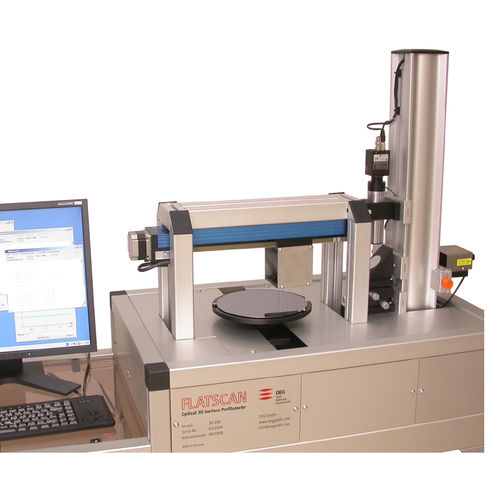
Non contact automated 2D- or 3D measurement of warp, bow, slope and surface curvature with software module for calculation of thin film stress (wafer stress) of wafers and glass substrates.
Application
FLATSCAN serves for the contactless measurement of flatness, waviness, mean radius and thin film stress of all kinds of reflecting surfaces like silicon wafers, mirrors, x-ray-mirrors (goebel-mirrors), metal surfaces or polished polymers. The optical measurement principle ensures a high accuracy. It is based on the measurement of the reflection angle of a perpendicular incident laser beam along a line with constant step width. The surface form can be calculated exactly from the change of the reflection angle from between the measuring points. For some applications the reflection angle itself is interesting. Therefore the software offers additionally this measuring option.
For applications in semiconductor technology the thin film stress in coatings can be calculated by the measured radii before and after coating.
Large measuring field
A special feature of the used measuring principle is its indpendence from the measuring field.
Therefore the standard measuring field diameter of 200mm can be increased nearly arbitrarily without decrease of accuracy.
High measuring accuracy
FLATSCAN is featured by a high measuring accuracy. The resolution of the measuring systems is 0,1 arcsec. The surface form reproducibility amounts to 100nm.
VIDEO
Catalogs
Related Searches
- Measuring device
- Measuring machine
- Automatic test equipment
- Optical measuring machine
- Automatic measuring machine
- Automatic measuring device
- Laboratory measuring device
- Diameter measuring machine
- Laser measurement system
- Geometry measuring device
- Thickness measurement system
- Optical measuring device
- Angle measuring machine
- PC-controllable testing device
- Process measuring device
- Measuring column
- Manual measuring device
- Non-contact measuring device
- Diameter gauge
- Flatness measuring machine
*Prices are pre-tax. They exclude delivery charges and customs duties and do not include additional charges for installation or activation options. Prices are indicative only and may vary by country, with changes to the cost of raw materials and exchange rates.


