- Production Machines
- Other Manufacturing Equipment
- Wafer inspection machine
- Onto Innovation Inc.
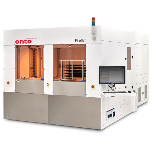
Wafer inspection machine Firefly® industrialfor the packaging industrymulti-function


Add to favorites
Compare this product
Characteristics
- Applications
- for wafers
- Sector
- industrial, for the packaging industry, multi-function
- Other characteristics
- defect, automated
Description
The Firefly inspection series provides an automated inspection solution for high performance applications like FPGA, CPU/GPU and networking servers in addition to applications with low I/O counts: IC drivers, RF transceivers, wireless connectivity and MEMS.
Product Overview
The platform, configurable for either wafer (round) or panel (rectangular) substrates, offers multiple imaging modes, including Onto Innovation’s patented Clearfind® Technology, a technique for enabling a large process window to detect residue defects on metal and metal defects on organic layers. The combination of substrate flexibility, defect sensitivity and metrology in a single platform reduces capital investment requirements and provides a reliable pathway to transition from wafer to panel-based processes for applications requiring high I/O counts and multiple-chip integration, such as SoC with memory, wireless module and wide I/O memory.
Integration with Onto Innovation’s Discover Defect software quickly turns defect data into actionable process control, improves classification and reduces manual review. It enables our customers to develop, learn and analyze new processes reliably while significantly improving their product delivery time to market.
Applications
Fan-out Wafer Level Packaging (FOWLP) / Fan-out Panel Level Packaging (FOPLP)
2.5D/Interposers
Embedded Die/Embedded Interposer
3DIC
MEMS
Image Sensors (CIS)
Front-end Macro for Advanced IC nodes
Related Searches
- Inspection machine
- Automatic inspection machine
- Industrial inspection machine
- Defect inspection machine
- Measurement inspection machine
- Visual inspection machine
- Surface inspection machine
- High-speed inspection machine
- Automated inspection machine
- High-resolution inspection machine
- Inspection machine for the packaging industry
- 3D inspection machine
- Sorting inspection machine
- Wafer inspection machine
- Multi-function inspection machine
- Lithography system
- Particle inspection machine
- Macro defect inspection machine
*Prices are pre-tax. They exclude delivery charges and customs duties and do not include additional charges for installation or activation options. Prices are indicative only and may vary by country, with changes to the cost of raw materials and exchange rates.


