- Materials - Tools - Components
- Semi-finished products
- Substrate for the electronics industry
- Panasonic Electric Works Corporation of America
- Products
- Catalogs
- News & Trends
- Exhibitions
Substrate for the electronics industry

Add to favorites
Compare this product
Characteristics
- Options
- for the electronics industry
Description
NEW SEMICONDUCTOR SUBSTRATE MATERIAL, R-1515V, IMPROVES ASSEMBLY-LEVEL RELIABILITY
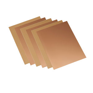
Panasonic's new semiconductor packaging material, R-1515V, enables both low package warpage and high assembly-level reliability. This new material has very low thermal expansion properties which reduces the warping of the substrate during the packaging process. Its optimized mechanical properties lower the residual stress on solder joints, created during reflow assembly, to improve reliability.
Suitable for IoT, V2X, 5G and other leading-edge technologies.
Panasonic's new substrate material improves package-level reliability by reducing warpage during packaging (mounting chips on the IC substrate followed by an encapsulation process). The coefficient of thermal expansion (CTE) of the new substrate material is much closer to that of silicon IC chips, reducing warpage caused by the thermal excursions during packaging processes.
During the reflow assembly process, when the semiconductor package is assembled onto the motherboard, the material lowers stress imparted to the solder balls - improving assembly-level reliability. The new material features excellent thickness tolerances, ensuring stable junctions between the substrate and the IC chips. This modified flexibility and buffering properties alleviate the stress on solder balls, improving the assembly-level reliability.
Low Thermal Expansion Coefficient (CTE) Close To That Of Silicon IC Chips Reduces Warping - Addressing A Critical Challenge With The IC Chip Packaging Process
Retaining Low Thermal Expansion Properties Through A Stress Relaxation Technology Improves The Reliability Pf The Assembly Process
Catalogs
No catalogs are available for this product.
See all of Panasonic Electric Works Corporation of America‘s catalogsOther Panasonic Electric Works Corporation of America products
Products
*Prices are pre-tax. They exclude delivery charges and customs duties and do not include additional charges for installation or activation options. Prices are indicative only and may vary by country, with changes to the cost of raw materials and exchange rates.


