- Production Machines
- Cutting Machine
- Plasma cutter
- Panasonic Factory Automation Company
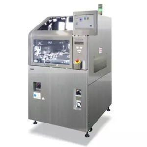
Plasma cutter APX300-DM
Add to favorites
Compare this product
Description
Plasma dicing is becoming increasingly attractive in the semiconductor market. Dies are becoming smaller and thinner and manufacturers are facing difficulties such as increasing material loss due to the width of the dicing line, mechanical damage to the dies from chipping and increasingly longer processing times due to line-by-line mechanical dicing.
Panasonic’s APX300-DM Plasma Dicer solves these challenges and simultaneously provides a higher quality product with a lower cost of production. Ideal for thin, brittle, and ultra-thin wafers; a damage-free, particle-free, stress-free and high die strength non-contact dicing and enabling ultra-narrow 20μm dicing street. Up to 300mm wafer and patented tape and frame protection from effects of plasma during dicing.
• Single chamber to scalable Cluster chamber option
• Particle-free and damage-free process
• Higher chip strength and yield improvements
• The Panasonic APX300 is CE certified
Process Gas - 4 Lines (standard) (Maximum 6 Lines: Chlorinated Gas, Fluoride Gas, Ar, O2, He, etc.)
Wafer Size * - φ100 mm wafer with orientation flat (standard)
[*1]
Dimensions (mm) - W 1,350 × D 2,230 × H 2,000 (Does not include touch panels, operation section and signal tower)
Mass - 2,100 kg (differs depending on machine configuration)
Power Source * - 3-phase AC 200 / 208 / 220 / 230 / 240 ±10 V, 50 / 60 Hz, 21.00 kVA
[*2]
Pneumatic Source - 0.5 MPa to 0.7 MPa, 250 L/min (A.N.R.)
N2 Source - 0.1 MPa to 0.2 MPa, 50 L/min (A.N.R.)
Catalogs
APX300-DM
2 Pages
Other Panasonic Factory Automation Company products
Microelectronics
Related Searches
*Prices are pre-tax. They exclude delivery charges and customs duties and do not include additional charges for installation or activation options. Prices are indicative only and may vary by country, with changes to the cost of raw materials and exchange rates.


