
- Products
- Catalogs
- News & Trends
- Exhibitions
Double-sided printed circuit board
Add to favorites
Compare this product
Characteristics
- Options
- double-sided
Description
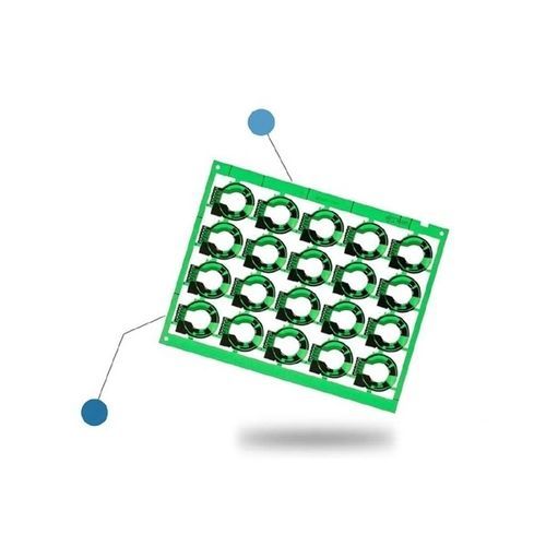
Single sided PCB ’s earliest industrial application can be traced back to the early 1950s. Because of its simple design principle and manufacturing process, it occupies an important position in the history of PCB manufacturing.
Single sided PCB is covered with copper on one side only, with components distributed on one side and circuits distributed on the other side. From top to bottom, single panel usually consists of soldermask layer, copper layer and insulating material in turn.
As only one side of single sided PCB can distribute circuits, and the two sides can't be connected, compared with other PCBs, they need a larger area to carry the same number of components, so they are more suitable for the design with lower requirements for component distribution density.
Although single layer PCB design is simpler than other types of PCB, based on the characteristics of single-sided distribution, it has stricter specifications for the design of wiring and component positions. For example, the pad of single sided PCB must be large, otherwise it is easy to cause problems during welding and repair. The wiring of the circuit board can not cross, but can only be designed along their own paths, etc.
Features of Single sided PCB
As only one side of single sided PCB can distribute circuits, and the two sides can't be connected, compared with other PCBs, they need a larger area to carry the same number of components, so they are more suitable for the design with lower requirements for component distribution density.
Related Searches
- PCBA
- Multilayer PCB
- Circuit board
- Double-sided PCB
- 2-layers printed circuit board
- 4-layers PCB
- 8 layers PCB
- 6 layers PCB
- High-frequency printed circuit board
- 10 layers printed circuit board
- 1 layer printed circuit board
- 14 layers printed circuit board
- 3 layers printed circuit board
- 5 layers printed circuit board
- Long printed circuit board
- 10 layers printed circuit board
- 20 layers printed circuit board
- 24 layers printed circuit board
- 40 layers printed circuit board
*Prices are pre-tax. They exclude delivery charges and customs duties and do not include additional charges for installation or activation options. Prices are indicative only and may vary by country, with changes to the cost of raw materials and exchange rates.


