
- Company
- Products
- Catalogs
- News & Trends
- Exhibitions
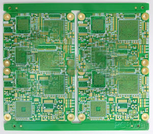
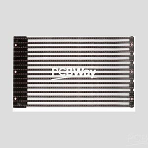
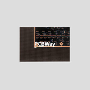
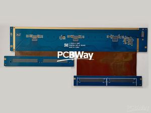
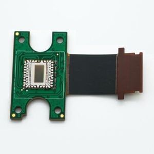
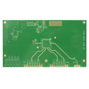
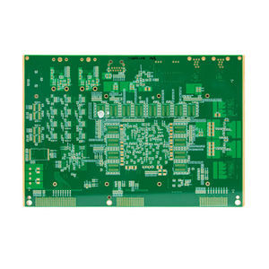
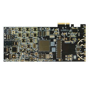
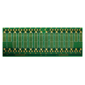
High-frequency printed circuit board 1 layer
Add to favorites
Compare this product
Characteristics
- Options
- high-frequency
- Number of layers
- 1 layer
Description
1.Up to 64 layer processing technology, the minimum trace and space is 2.5 / 2.5mil, the highest ratio of board thickness and hole diameter is 16:1.
2. Long and short gold finger processing technology and high-density trace’s precision control to meet the design requirements of photoelectric communication products.
3. High-precision back-drilling technology to reduce the equivalent series inductance of vias and in case to meet the product’s integrity requirements of signal transmission;
4. Advanced metal-based and ultra-thick copper manufacturing process to meet the high heat dissipation requirements of power products.
5. High-precision mechanical and laser depth control technology to achieve multi-level step groove product’s structure and meet the different levels of assembly requirements.
6. The mature mixed pressure process realizes the mixing of FR-4 and high-frequency materials, and saves the material cost for customers under the premise of achieving the high-frequency performance of the products.
7. Advanced Anti-CAF process technology greatly improves the reliability and service life of PCB products.
8. Advanced buried capacitor and buried resistor technology greatly improve the performance of PCB products.
9. Advanced inner layer exposed technology meets the information transmission requirements of high frequency circuits.
Advanced Processing And Testing Equipment
1.Orbotech AOI (automatic optical inspection) machine imported from Israel for detecting high-precision circuits.
2.The high-precision impedance tester imported from the United States meets the impedance test requirement.
Catalogs
No catalogs are available for this product.
See all of PCBWay‘s catalogsRelated Searches
- PCBA
- Multilayer PCB
- Double-sided PCB
- Communication module PCB
- 2-layers printed circuit board
- 4-layers PCB
- 8 layers PCB
- Electronic PCB
- 6 layers PCB
- High-frequency printed circuit board
- PCBA for automotive applications
- 10 layers printed circuit board
- PCB for industrial applications
- PCBA for medical applications
- 5G antenna printed circuit board
- 1 layer printed circuit board
- High-speed printed circuit board
- 14 layers printed circuit board
- 3 layers printed circuit board
- 16 layers printed circuit board
*Prices are pre-tax. They exclude delivery charges and customs duties and do not include additional charges for installation or activation options. Prices are indicative only and may vary by country, with changes to the cost of raw materials and exchange rates.

