- Metrology - Laboratory
- Inspection and Monitoring
- Wafer camera
- Photonic Science and Engineering
Wafer camera machine visioninfraredInGaAs

Add to favorites
Compare this product
Characteristics
- Applications
- for wafers
- Function
- machine vision
- Spectrum
- infrared
- Other characteristics
- InGaAs
Description
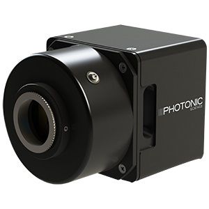
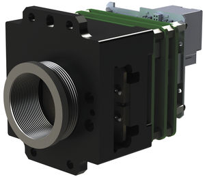
InGaAs short wave infrared SWIR cameras deliver 640x512 resolution with response up to 1.7 µm.
The high resolution SWIR camera can be used for a very wide variety of applications including laser beam profiling, semiconductor inspection, hyperspectral imaging, on-line process control, Low-light level imaging, and screening solar cells.
For solar cells screening, defects at early processing stage can be imaged through the bulk silicon thanks to its transparency at wavelengths beyond 1.1 µm. Cracks, dead or weak responding areas are unveiled on sliced wafers, enabling automatic sorting / selection of the best pieces. The camera finally captures faint electroluminescence (EL) and photoluminescence (PL) emissions from individual photovoltaic cells that are directly proportional to their efficiency.
Photonic Science high resolution SWIR cameras can be supplied with state of art SWIR optics which will deliver superior resolution / contrast modulation and lower distortion than conventional NIR optics that are used with conventional CCD cameras.
Key Features
- 14-bit digitization / 16-bit image processing
- Read out noise
- down to typically 200 fps
- With Region of Interest ROI
- Excellent linearity
- Response to varying intensities and/or exposures
- Gigabit Ethernet & Camera Link interface
- Software option
- SDK kit, Labview VI’s
Catalogs
No catalogs are available for this product.
See all of Photonic Science and Engineering‘s catalogsOther Photonic Science and Engineering products
SWIR / InGaAs cameras
Related Searches
- Digital camera module
- Visible camera system
- CMOS camera module
- Industrial camera system
- Infrared imager
- Surveillance camera
- Full-color camera system
- Vision processing camera
- Monochrome video camera
- Thermal camera
- High-definition camera
- Gigabit Ethernet camera
- High-speed camera system
- CCD video camera
- Spark optical emission camera system
- Machine vision camera module
- High-sensitivity imager
- Full HD camera module
- Low light camera
- Camera Link camera module
*Prices are pre-tax. They exclude delivery charges and customs duties and do not include additional charges for installation or activation options. Prices are indicative only and may vary by country, with changes to the cost of raw materials and exchange rates.


