- Electricity - Electronics
- Electronic Component
- Switching regulator
- Power Integrations
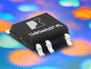
High-efficiency switching regulator 700 V | LinkSwitch-IIlow-power
Add to favorites
Compare this product
Characteristics
- Options
- high-efficiency, low-power
Description
The LinkSwitch-II dramatically simplifies low power CV/CC charger designs by eliminating an optocoupler and secondary control circuitry. The device introduces a revolutionary control technique to provide very tight output voltage and current regulation, compensating for transformer and internal parameter tolerances along with input voltage variations.
The device incorporates a 700 V power MOSFET, a novel On/Off control state machine, a high voltage switched current source for self biasing, frequency jittering, cycle-by-cycle current limit and hysteretic thermal shutdown circuitry onto a monolithic IC.
VIDEO
Catalogs
No catalogs are available for this product.
See all of Power Integrations‘s catalogsRelated Searches
- Capacitor
- Diode
- Transistor module
- SMD capacitor
- LED driver
- High-speed switching diode
- MOSFET transistor module
- Power IC converter
- Adjustable LED driver
- Dimmable LED driver
- PN junction diode
- Gate driver
- Switching regulator
- Power IC
- Digital IC
- Switching diode
- Radial-lead diode
- IC LED driver
- IGBT gate driver
- Constant-current LED driver
*Prices are pre-tax. They exclude delivery charges and customs duties and do not include additional charges for installation or activation options. Prices are indicative only and may vary by country, with changes to the cost of raw materials and exchange rates.


