- Electricity - Electronics
- Electronic Component
- Power microchip
- Power Integrations
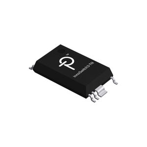
Power IC LinkSwitch-TNZ seriesMOSFET
Add to favorites
Compare this product
Characteristics
- Options
- power, MOSFET
Description
The LinkSwitch-TNZ family of ICs combine power conversion with lossless generation of AC zero crossing signal used typically for system clock and timing functions. Designs using the highly integrated LinkSwitch-TNZ ICs are more flexible than discrete implementations reducing component count by 40% or higher. Besides enabling 80+ efficiencies in low power Flyback designs, very low consumption at light loads enabled by On/Off control allow for more functions (display, wireless connectivity, sensors etc.) to be active during system standby. The device family supports buck, buck-boost and flyback converter topologies.
Each device incorporates a 725 V power MOSFET, oscillator, a high-voltage switched current source for self-biasing, frequency jittering, fast (cycle-by-cycle) current limit, hysteretic thermal shutdown, and output and input overvoltage protection circuitry onto a monolithic IC.
LinkSwitch-TNZ ICs consume <100 µA current in standby resulting in power supply designs that can meet no-load and standby regulations worldwide. MOSFET current limit modes can be selected through the BYPASS pin capacitor value. The high current limit level provides maximum continuous output current while the low level permits using very low-cost and small surface mount inductors. A full suite of protection features enables safe and reliable power supplies protecting the device and the system against input and output overvoltage faults, device over-temperature faults, lost regulation, and power supply output overload or short-circuit faults.
Lossless zero cross signal generation
Supports buck, buck-boost and flyback topologies
Enables ±3% regulation across line and load
Catalogs
No catalogs are available for this product.
See all of Power Integrations‘s catalogsRelated Searches
- Capacitor
- Diode
- Transistor module
- SMD capacitor
- LED driver
- High-speed switching diode
- MOSFET transistor module
- Power IC converter
- Adjustable LED driver
- Dimmable LED driver
- PN junction diode
- Gate driver
- Switching regulator
- Power IC
- Digital IC
- Switching diode
- Radial-lead diode
- IC LED driver
- IGBT gate driver
- Constant-current LED driver
*Prices are pre-tax. They exclude delivery charges and customs duties and do not include additional charges for installation or activation options. Prices are indicative only and may vary by country, with changes to the cost of raw materials and exchange rates.


