
- Products
- Catalogs
- News & Trends
- Exhibitions
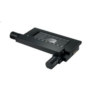
Microscope positioning stage H112XYmotorized2-axis
Add to favorites
Compare this product
Characteristics
- Orientation
- XY
- Type
- motorized
- Number of axes
- 2-axis
- Other characteristics
- industrial, for microscopes, long-travel, with built-in stepper motor
- Stroke
302 mm
(11.89 in)- Speed
40 mm/s
- Repeatability
0.7 µm
- Load
Max.: 25 kg
(55.12 lb)Min.: 0 kg
(0 lb)
Description
The H112/2ST stage is designed for scanning semiconductor wafers, photo masks, flat panel displays and printed circuit boards up to 300 mm (12-inch) diameter. Additionally, the stage supports a 25 kg load capacity making it capable of accurately positioning large and complex industrial samples over this large travel range. Transmitted light applications, such as infrared scanning of wafers, are also supported up to 250 mm diameter. Its slim and lightweight design enables easier integration into customized microscopes. Featuring Prior's patented Intelligent Scanning Technology (IST) to optimize stage accuracy, linearity and other performance characteristics, in combination with a 2 mm ballscrew for speed, the H112/2ST is optimized for scanning very large industrial samples reliably and efficiently. Alternative drive configurations for further increased speed may be available depending on your region. This stage can also be mounted onto large format Nikon and Evident/Olympus microscopes, and is compatible with Nikon and Evident/Olympus software (appropriate package required).
Catalogs
No catalogs are available for this product.
See all of Prior Scientific‘s catalogsRelated Searches
- Stage
- Linear stage
- Motorized stage
- Precision stage
- 1-axis stage
- 2-axis stage
- XY stage
- High-accuracy stage
- Industrial stage
- Ball screw stage
- Vertical stage
- Miniature stage
- Linear motor-driven stage
- Microscope stage
- Heavy load stage
- Measurement stage
- Stage with ball bearing
- Long-travel stage
- Low-profile stage
- Nanopositioning stage
*Prices are pre-tax. They exclude delivery charges and customs duties and do not include additional charges for installation or activation options. Prices are indicative only and may vary by country, with changes to the cost of raw materials and exchange rates.


