- Company
- Products
- Catalogs
- News & Trends
- Exhibitions
Stationary thickness gauge SK-FTM-Map seriesfilmspectral reflectanceautomatic calibration
Add to favorites
Compare this product
Characteristics
- Type
- stationary
- Applications
- film
- Technology
- spectral reflectance
- Calibration
- automatic calibration
- Measuring range
300 mm
(11.81 in)
Description
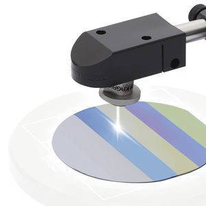
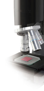
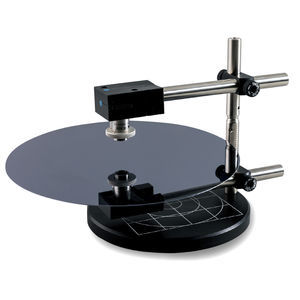
The wafer mapping unit is capable of automatic mapping film thickness measurement over the entire surface of wafers up to 300 mm. The automatic alignment function, self-calibration function and high flatness wafer chuck enable highly reliable film thickness measurement. This unit is used in combination with the compact film thickness monitor.
It can be installed at the load port of semiconductor manufacturing equipment to control the film thickness on the manufacturing equipment while maintaining cleanliness.
1 Automatic film thickness mapping measurement of up to 300 mm wafer is possible
2 Automatic alignment function
3 Automatic calibration function
4 Improved measurement reliability in the wafer surface by adopting a wafer chuck with high flatness
5 Supports automation
6 Load port installation
Catalogs
No catalogs are available for this product.
See all of Shashin Kagaku‘s catalogs*Prices are pre-tax. They exclude delivery charges and customs duties and do not include additional charges for installation or activation options. Prices are indicative only and may vary by country, with changes to the cost of raw materials and exchange rates.


