- Electricity - Electronics
- Electronic Component
- Electronic printed circuit board
- Shenzhen STHL Technology Co.,Ltd
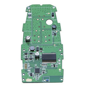
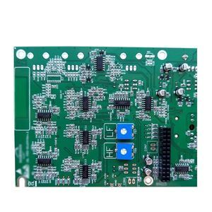
Universal printed circuit for electronics


Add to favorites
Compare this product
Characteristics
- Options
- universal
- Applications
- for electronics
Description
What is Multilayer PCB?
A multilayer PCB consists of three or more layers of conductive copper foils, compared to the traditional single-layer PCB which has only one layer. A double-sided PCB has two conductive layers on the top and bottom of the PCB substrate. The top and bottom layers of a multilayer PCB resemble those of a double-sided PCB, but there are additional layers on both sides of the core. They are typically made by laminating multiple layers of double-sided circuit boards together with layers of heat-protective insulations. Copper-plated holes interconnect these layers, and electrical connections between the middle layers are achieved through vias such as blind and buried vias, and plating through holes.
On the top and bottom layers of the multilayer PCB, active and passive components are placed, while the inner stacked layers are used for routing. It is arranged so that on the PCB, two layers are placed on the surface to connect the environment. Both through-hole electronic components and Surface Mount Components (SMD) can be soldered on either side of this type of PCB. SMD components can be soldered using Surface Mount Technology and other PCBA Tools. By applying such methods, manufacturers can construct highly complex PCBs of different sizes. Multilayer PCBs can have up to 40 layers.
Catalogs
No catalogs are available for this product.
See all of Shenzhen STHL Technology Co.,Ltd‘s catalogsOther Shenzhen STHL Technology Co.,Ltd products
SMT Assembly
Related Searches
- PCB
- Multilayer PCB
- Flexible printed circuit
- Double-sided PCB
- Communication module PCB
- 2-layers printed circuit board
- 4-layers PCB
- Custom PCB
- 8 layers PCB
- Electronic printed circuit board
- 6 layers PCB
- High-frequency printed circuit board
- PCB for automotive applications
- PCB for industrial applications
- PCB for medical applications
- Telephone printed circuit board
*Prices are pre-tax. They exclude delivery charges and customs duties and do not include additional charges for installation or activation options. Prices are indicative only and may vary by country, with changes to the cost of raw materials and exchange rates.


