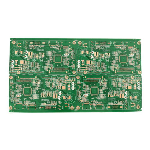
Archecircuit Multilayer PCB OSP for Networking and Communication System
Dimension: 270.00*150.00 mm
Plate thickness: 1.6mm
Plate: FR-4
Surface finish: OSP
Application: Networking & Commnunication
Material - FR-4 (Tg 135 / Tg140 / Tg155 / Tg170/ As you required)
Aluminum
Rogers / PTFE Teflon
Surface Finishing - HASL/OSP/Immersion Gold(FR4)
HASL(Aluminum)
Printed Wiring: - Pattern Plating
Max. Dimension - 660×475mm
Min. Dimension - 5×5mm
Finished board thickness: - 0.2mm-3.0mm
Thickness Tolerance:
( Thickness≥1.0mm) - ± 10%
Thickness Tolerance:
( Thickness<1.0mm) - ± 0.1mm
Finished Outer Layer Copper - Double sided: 1 oz/2 oz/3 oz/4 oz
Multilayer: 1 oz/2 oz
Finished Inner Layer Copper - 0.5 oz/1 oz/2 oz
Drill Hole Size - Double sided: 0.20mm – 6.30mm
Multilayer: 0.15mm-6.3mm
Drill Hole Size Tolerance - Pad Hole: +0.13/-0.08mm
Pressure Welding Hole: ±0.05mm
Blind/Buried Vias - Don’t support
Min. Via Hole Size/Diameter - 1 & 2 Layer: 0.3mm(Via hole size) / 0.5mm(Via diameter)
Multi-Layer: 0.15mm(Via hole size) / 0.25mm(Via diameter)
Via diameter should be 0.1mm(0.15mm preferred) larger than Via hole size
Preferred Min. Via hole size: 0.2mm
Min. Plated Slots - 0.35mm
Min. Non-Plated Slots - 0.65mm


