Design software 3D IC design solutionsanalysisprototypingdevelopment
Add to favorites
Compare this product
Characteristics
- Function
- analysis, development, design, planning, optimization, verification, prototyping, co-simulation
- Applications
- process, flow
- Type
- 3D, automated
Description
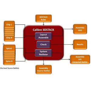
An integrated IC packaging solution that covers everything from planning and prototyping to signoff for various integration technologies such as FCBGA, FOWLP, 2.5/3D IC, and others. Our 3D IC packaging solutions help you overcome the limitations of monolithic scaling.
What is 3D IC technology?
The semiconductor industry has made great strides in ASIC technology over the last 40 years, leading to better performance. But as Moore's law nears its limits, scaling devices is becoming harder. Shrinking devices now takes longer, costs more, and presents challenges in technology, design, analysis, and manufacturing. Thus, enters 3D IC.
Key benefits for Siemens 3D IC design flow tools
Tackle 3D IC integration and packaging with system co-optimization to balance requirements and resources and gain visibility into downstream impact to PPA and cost.
3D IC digital transformation
Enable digital transformation for 3D chip design with co-design, co-simulation and automated system analysis and checking. Replace manual interfaces and data exchanges with automated methods and defined workflows.
3D IC verification and validation
Comprehensive 3D IC packaging coverage for performance validation and design verification from predictive to final sign off. Automated reviews identify overt issues earlier in the chip design process and eliminate iterations.
Better 3D IC design resource utilization
Support team-based design for concurrent development and enable IP reuse and managed blocks. Leverage one chiplet layout tool for organic and silicon substrates for better advanced packaging design.
Catalogs
No catalogs are available for this product.
See all of SIEMENS EDA‘s catalogsRelated Searches
- Automation software solution
- Management software solution
- Analysis software solution
- Process software solution
- Windows software solution
- Computer-aided design software
- Control software solution
- Real-time software solution
- Online software
- Design software solution
- 3D software solution
- Measurement software
- Interface software
- Industrial software solution
- Quality software
- Simulation software
- Visualization software solution
- Automated software
- Development software
- Network software solution
*Prices are pre-tax. They exclude delivery charges and customs duties and do not include additional charges for installation or activation options. Prices are indicative only and may vary by country, with changes to the cost of raw materials and exchange rates.


