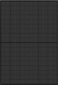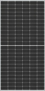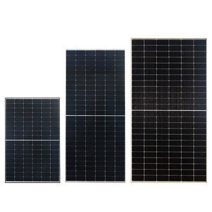
Monocrystalline silicon solar module EN_STP420-440S-C54-NshmCEISOIEC
Add to favorites
Compare this product
Characteristics
- Technology
- monocrystalline silicon
- Certifications
- CE, IEC, ISO
- Other characteristics
- black
- Peak power (Wp)
415 W, 420 W, 425 W, 430 W, 435 W
- Open-circuit voltage
38.3 V, 38.5 V, 38.6 V, 38.7 V, 38.9 V
- Short circuit current
14 A, 14.1 A, 14.2 A, 14.3 A
- Max power voltage
31.8 V, 32 V, 32.2 V, 32.3 V, 32.5 V
- Max power current
13.1 A, 13.2 A, 13.3 A, 13.4 A
- Module efficiency
21.3 %, 21.5 %, 21.8 %, 22 %, 22.3 %
- Lenght
1,722 mm
(68 in)- Width
1,134 mm
(45 in)- Height
30 mm
(1 in)- Weight
21 kg
(46.3 lb)
Description
Large format 210 mm silicon wafers with the module efficiency up to 21.6%
Based on 210 mm large format silicon wafer and PERC monocrystalline cell, increase light receiving area by 80.5% compared with 156mm cell, the conversion efficiency is greatly improved.
With Suntech’s non-destructive cutting technology, avoid the damage of cutting surface, realize the optimal half-cell design, and reduce the current loss and the risk of hot spot.
MBB technology + High-density packaging technology, the maximum power breaks through 670 W
With multi-busbar technology, the transverse propagation path of the current decreases by 50%, reduce resistance loss effectively, realize the maximum power output, meanwhile, and assure the reliability of the module.
Suntech adopts high-density packaging technology on Ultra X module, which can shorten distance between the cells and decrease the invalid power generation area greatly, and improves the energy density of the module.
The upgraded high efficiency welding strip, lead to more second time refection of oblique light, increase the power generation by 1.57%.
With the unique layout design, the weight of module is reduced by 20%
Suntech has particularly optimized structure design, with exclusive patent, module weighs 31.5 KG,It has super mechanical load capacity and the load can reach up to +5400/-2400 Pa,the maximum deformation is reduced by 37%, then avoid the risk of micro crack loss.
Catalogs
No catalogs are available for this product.
See all of Suntech Power Corporation‘s catalogs*Prices are pre-tax. They exclude delivery charges and customs duties and do not include additional charges for installation or activation options. Prices are indicative only and may vary by country, with changes to the cost of raw materials and exchange rates.


