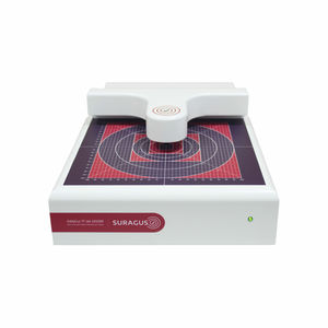
Bench-top conductivity meter EddyCus® TF map 2525RM

Add to favorites
Compare this product
Characteristics
- Type
- bench-top
Description
EddyCus® TF map 2525RM – Conductivity Mapping and Defect Identification in Thin Films
A variety of materials characteristics determine the conductivity of materials. Next to its composition also its structure and its purity affect the conductivity. The EddyCus® TF map 2525RM is an eddy current mapping system dedicated to high-resolution imaging of conductivity and correlated characteristics exposing material properties, effects and defects. The system can be equipped with various EddyCus sensors for conductivity imaging in high resolution or high penetration and defect detection by use of differential probes. The system supports the creation of images (Eddy Current C-Scans) of the surface with a measurement pitch of 100 µm to 10 mm. The three axis system is capable to scan 2D and 2.5D areas with a size of up to 250 x 250 mm / 10 x 10 inch. Typical applications cover the surface characterization of conductive materials such as SiC-, Graphite-, metal, alloy or steel plates or other conductive semi-finished products. Additionally, the system can be used for testing the electrical integrity of printed electronics and layers.
Eddy current testing allows the quantification of material conductivity [IACS or MS/m] or resistivity [Ohm m or Ohm / mm² / m]. The conductivity of materials provides information on material characteristics such as type of material and homogeneity of the material composition. Next to the direct information on electrical properties, the conductivity also contains information that relate to its thermic properties or its mechanical properties and its structural integrity.
VIDEO
Catalogs
No catalogs are available for this product.
See all of SURAGUS GmbH‘s catalogsRelated Searches
*Prices are pre-tax. They exclude delivery charges and customs duties and do not include additional charges for installation or activation options. Prices are indicative only and may vary by country, with changes to the cost of raw materials and exchange rates.


