- Machine-tools
- Machining Center
- Laser micro-machining machine
- SUZHOU CHANXAN LASER TECHNOLOGY CO., LTD.
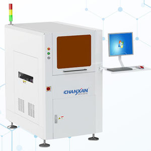
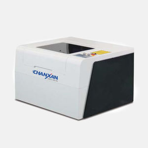
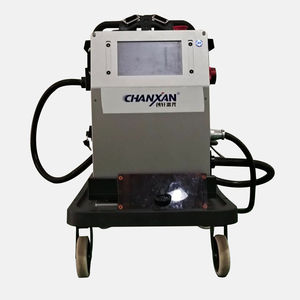
Laser micro-machining machine CS-0605-V seriesfor metalscutting
Add to favorites
Compare this product
Characteristics
- Type
- laser
- Machined material
- for metals
- Associated functions
- cutting
Description
Widely used in semiconductor integrated circuits, including single and double mesa glass passivation diode wafer cutting and dicing, single and double mesa thyristor wafer cutting and dicing, gallium arsenide, gallium nitride, IC wafer cutting and dicing.
Principle of picosecond laser scribing (focus burst cutting in transparent material):
Through the Bessel or DOE optical system, the Gaussian laser beam is compressed to the diffraction limit. Under the action of the laser beam with a high repetition rate of 100-200KHz and a very short pulse width of 10ps, the focused spot diameter is as small as 3μm, and it has a very high peak power. Density, when it is focused inside the transparent material, it instantly vaporizes the material in the area to generate a vaporization zone, and diffuses to the upper and lower surfaces to form nonlinear cracks, thereby realizing the cutting and separation of the material. Common transparent materials including glass, sapphire and semiconductor silicon wafers (infrared radiation is able to transmit semiconductor silicon materials) are suitable for picosecond & femtosecond laser scribing.
Features
Multiple laser operation modes and beam shaping to ensure incision quality and efficiency
Unique wavefront correction technology ensures high precision machining and consistency
Automatic positioning, automatic focusing, automatic detection to ensure production yield
It can realize automatic slitting or manual slitting selection of large graphics, and the splicing accuracy is as high as ±1um
Support warping film, TAIKO film transfer film
Other SUZHOU CHANXAN LASER TECHNOLOGY CO., LTD. products
Laser Precision Processing
*Prices are pre-tax. They exclude delivery charges and customs duties and do not include additional charges for installation or activation options. Prices are indicative only and may vary by country, with changes to the cost of raw materials and exchange rates.


