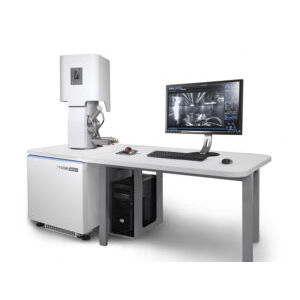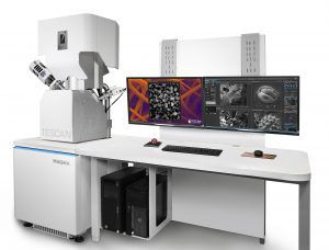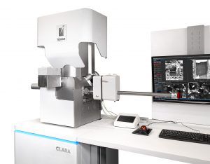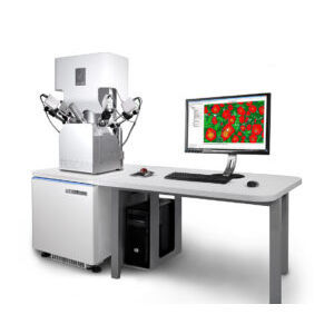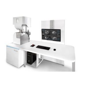
SEM microscope CLARAfor materials inspectionbenchtopautomated
Add to favorites
Compare this product
Characteristics
- Type
- SEM
- Technical applications
- for materials inspection
- Configuration
- benchtop
- Other characteristics
- automated, modular
Description
Field-free analytical UHR SEM for materials characterization at nanoscale
• Uncompromised characterization of all types of materials at the nanoscale
• Ideal for characterization of materials at low beam energies for maximum surface topography
• Excellent imaging of beam-sensitive and non-conductive samples
• Fully automated setup of electron beam – optimal imaging conditions are guaranteed by the In-Flight Beam Tracing™
• Intuitive live SEM navigation on the sample at magnification as low as 2× without the need of extra optical navigation camera thanks to the Wide Field Optics™ design
• Unique In-Beam Multidetector design allowing angle and energy selective BSE detection
• Intuitive software modular platform designed for effortless operation regardless of users’ skill level
Catalogs
No catalogs are available for this product.
See all of Tescan GmbH‘s catalogsRelated Searches
- Microscope
- Laboratory microscope
- Inspection microscope
- Tabletop microscope
- Measuring microscope
- Analysis microscope
- High-resolution microscope
- Industrial microscope
- Automatic microscope
- Materials research microscope
- Quality control microscope
- Research microscope
- Modular microscope
- Confocal microscope
- High-precision microscope
- Real-time microscope
- SEM microscope
- High-contrast microscope
- Secondary electron microscope
- Materials inspection microscope
*Prices are pre-tax. They exclude delivery charges and customs duties and do not include additional charges for installation or activation options. Prices are indicative only and may vary by country, with changes to the cost of raw materials and exchange rates.


