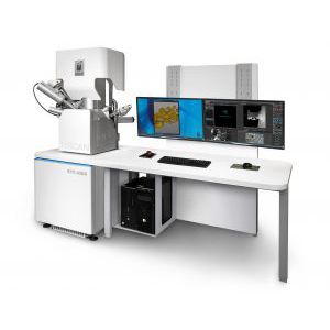
FIB/SEM microscope SOLARIS Xfor analysishigh-resolutionultra-high resolution
Add to favorites
Compare this product
Characteristics
- Type
- FIB/SEM
- Technical applications
- for analysis
- Other characteristics
- high-resolution, ultra-high resolution
Description
A Plasma FIB-SEM platform for deep sectioning and the highest resolution end-pointing for package level failure analysis
• Curtaining-free large-area cross-sectioning for physical failure analysis of advanced packaging technologies
• Prepare large area FIB-cross-sections up to 1 mm wide
• Obtain low noise, high-resolution image at low keVs in short acquisition time at FIB-SEM coincidence with the sample tilted
• Live SEM-monitoring during FIB milling for precise end-pointing
• Observe the most beam-sensitive materials using low keVs ultra-high resolution for surface sensitivity and high material contrast
• Effective techniques and recipes for fast and artefact-free cross-sectioning of composite samples (OLED and TFT displays, MEMS devices, isolation dielectrics) at high currents
• Essence™ easy-to-use modular user interface
Catalogs
No catalogs are available for this product.
See all of Tescan GmbH‘s catalogsRelated Searches
- Microscope
- Laboratory microscope
- Inspection microscope
- Tabletop microscope
- Measuring microscope
- Analysis microscope
- High-resolution microscope
- Industrial microscope
- Automatic microscope
- Materials research microscope
- Quality control microscope
- Research microscope
- Modular microscope
- Confocal microscope
- High-precision microscope
- Real-time microscope
- SEM microscope
- High-contrast microscope
- Secondary electron microscope
- Materials inspection microscope
*Prices are pre-tax. They exclude delivery charges and customs duties and do not include additional charges for installation or activation options. Prices are indicative only and may vary by country, with changes to the cost of raw materials and exchange rates.


