- Packing - Handling - Logistics
- Conveying
- Automatic sorter
- TZTEK Technology Co.,ltd
Automatic sorting system for waferssurface inspectionhigh-speed
Add to favorites
Compare this product
Characteristics
- Operational mode
- automatic
- Product applications
- for wafers, surface inspection
- Other characteristics
- high-speed
Description
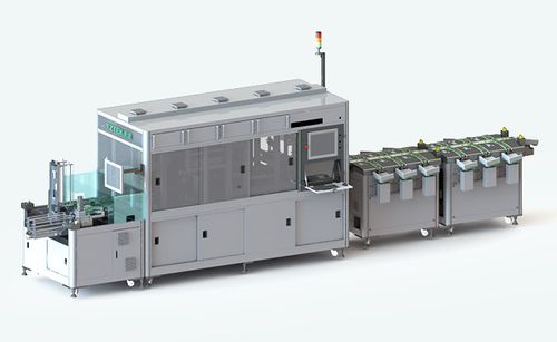
Photovoltaic Silicon wafer détection and sorting equipment can comprehensively test the quality of photovoltaic Silicon wafers, making it a key piece of equipment for photovoltaic Silicon wafer manufacturing.
The photovoltaic Silicon wafer détection and sorting equipment developed by TZTEK, integrating more than 10 years of machine vision technology and expérience, realizes one-step, high-speed, comprehensive détection and grading of dimensions, line marks, warpage, breakage, surface defects, latent cracks, electrical properties, and other characteristics of monocrystal, polycrystal, and black Silicon wafers by incorporating a deep learning Al algorithm. Specifically, it performs récognition and extraction with high efficiency and a high récognition rate of the characteristics of defects in Silicon wafers, and intégrâtes four major processes in quality control of Silicon wafers, including feeding, full détection, data analysis, and blanking & sorting, into an automatic intelligent System, so as to meet your requirements for sorting and détection of Silicon wafers and similar products in the new energy sector.
"0" Damage
Non-contact with "0” damage
Data Support
automatically collectiing and uploading real-time inspection and sorting data
Low Cost
Less labour investment, lower total sorting and testing costs
*Prices are pre-tax. They exclude delivery charges and customs duties and do not include additional charges for installation or activation options. Prices are indicative only and may vary by country, with changes to the cost of raw materials and exchange rates.


